

Fixing a pixel defect in display device
a display device and defect technology, applied in the field of fixing pixel defects, can solve the problems of degrading display quality, forming white spots, and oled often getting defective pixels, and achieve the effect of easy repair
- Summary
- Abstract
- Description
- Claims
- Application Information
AI Technical Summary
Benefits of technology
Problems solved by technology
Method used
Image

Examples
first embodiment
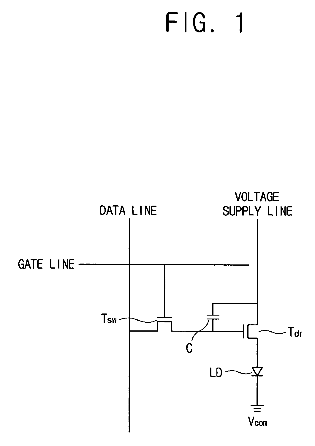
[0027]FIG. 1 is an equivalent circuit diagram of a pixel in a display device according to the present invention.
[0028] A pixel has a plurality of signal lines. The signal lines include a gate line transmitting a scan signal, a data line transmitting a data signal, and a voltage supply line transmitting a driving voltage. The data line and the voltage supply line are disposed parallel to each other, and the gate line extends perpendicularly to the data line and the voltage supply line.
[0029] Each pixel comprises a light emitting diode element LD, a switching thin film transistor Tsw, a driving thin film transistor Tdr, and a capacitor C.
[0030] The driving thin film transistor Tdr has a control terminal, an input terminal, and an output terminal. The control terminal is connected to the switching thin film transistor Tsw, the input terminal is connected to the voltage supply line, and the output terminal is connected to the light emitting diode element LD.
[0031] The light emitting ...
second embodiment
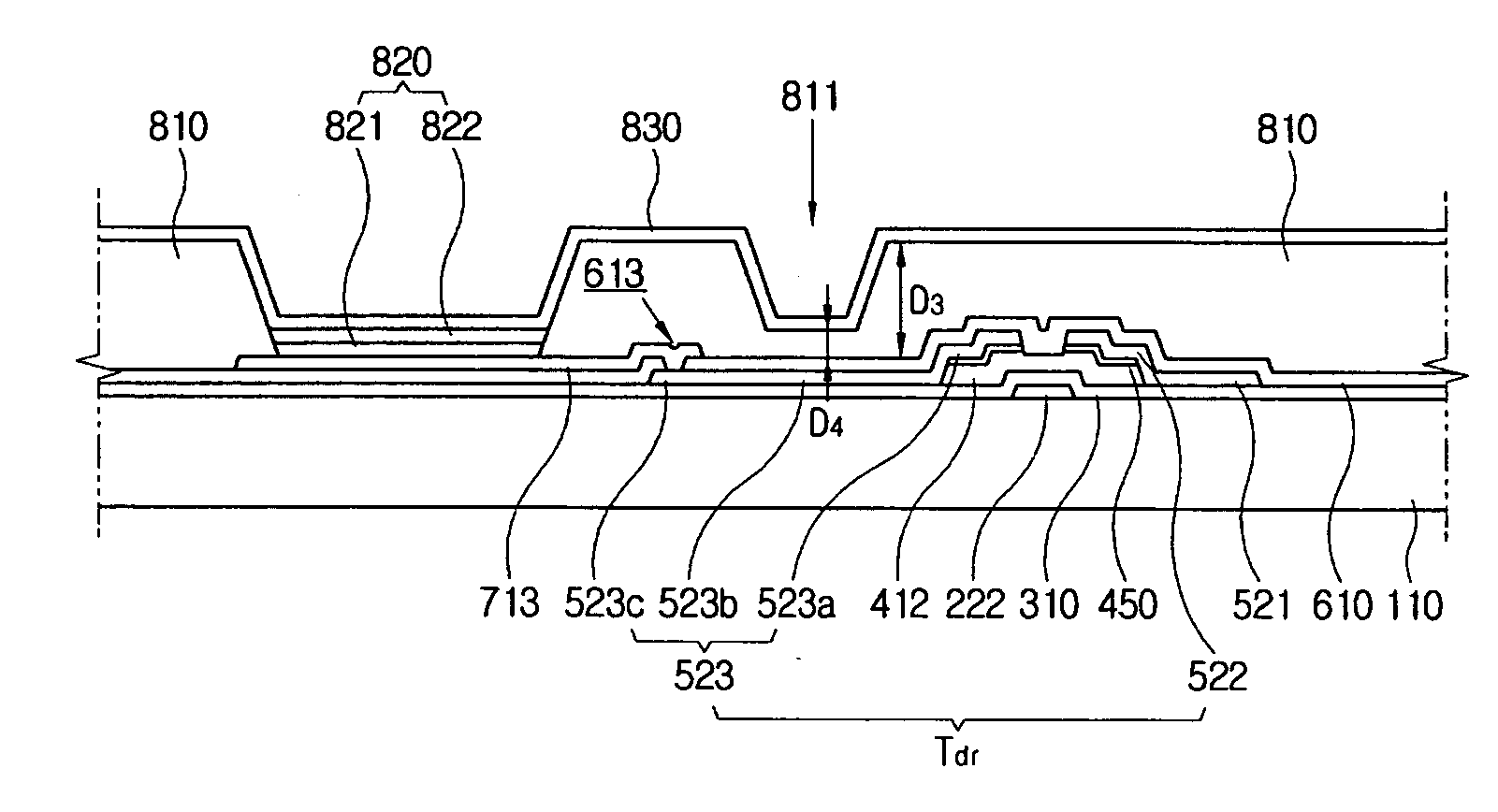
[0091] Hereinafter, a display device according to the present invention will be described with reference to FIGS. 7 and 8.
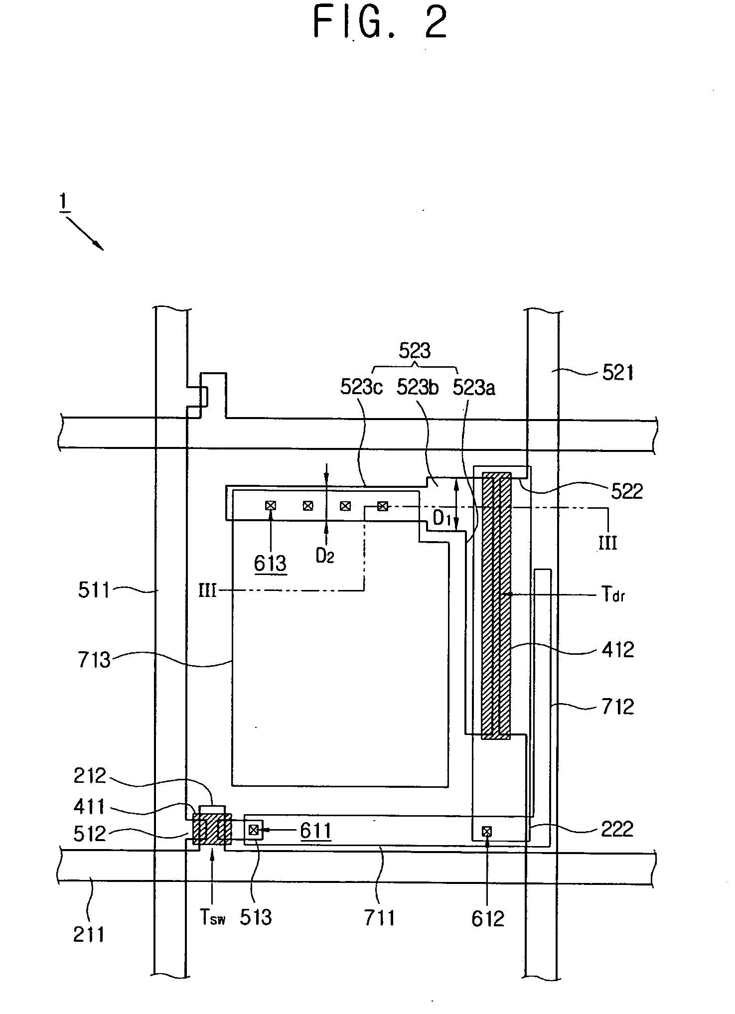
[0092]FIG. 7 is an arrangement view of the display device according to the second embodiment of the present invention, and FIG. 8 is a sectional view taken along the line VIII-VIII in FIG. 7.
[0093] In the second embodiment, the width d5 of a second part 523b of a driving drain electrode 523 is shorter than the width d2 of a third part 523c thereof. In detail, the width d5 of the second part 523b may be in the range of 50% and 90% of the width d2 of the third part 523c. The second part 523b in the second embodiment is to be irradiated with laser when repairing a pixel.
[0094]FIGS. 9A and 9B are sectional views to illustrate how to repair a defective pixel in the display device according to the second embodiment of the present invention.
[0095]FIG. 9A shows that the second part 523b of the driving drain electrode 523 is irradiated with laser to repair the pixel, a...
PUM
| Property | Measurement | Unit |
|---|---|---|
| Fraction | aaaaa | aaaaa |
| Fraction | aaaaa | aaaaa |
| Fraction | aaaaa | aaaaa |
Abstract
Description
Claims
Application Information