Thin film transistor substrate for display

a thin film transistor and substrate technology, applied in the field of conductive structure for use in thin film transistors, can solve the problems of affecting the performance of tft, copper has poor adhesion to insulting substrates, and delay the transference of signals, so as to achieve the effect of reliable patterning

Inactive Publication Date: 2007-05-31
SAMSUNG ELECTRONICS CO LTD
View PDF9 Cites 61 Cited by
  • Summary
  • Abstract
  • Description
  • Claims
  • Application Information

AI Technical Summary

Problems solved by technology

As the size of an LCD apparatus or OLED increases, the gate lines and data lines become longer and their electrical resistance increases thereby delaying the transference of signals.
However, copper has poor adhesion to insulting substrates such as to a glass substrate or a semiconductor layer.
Furthermore, copper ions rapidly defuse into an amorphous silicon (a-Si) or silicon (Si) layer when a TFT is operated and copper ions generated by the etchant (or etching solution) used in etching the conductive structure, or during stripping of the photo resist pattern may penetrate an amorphous silicon layer to create leakage currents affecting the performance of the TFT.
Additionally, silicon ions can also diffuse into a copper conductive structure raising its resistivity and lowering its chemical resistance to corrosion.
However, copper layer may be corroded by a galvanic effect arising during etching / patterning of the multi-layered structure or during the stripping of the photo resist pattern to causing an undesired overhang of the capping layer and defective side profile.

Method used


Image

  • Thin film transistor substrate for display
  • Thin film transistor substrate for display
  • Thin film transistor substrate for display

Examples


Embodiment Construction

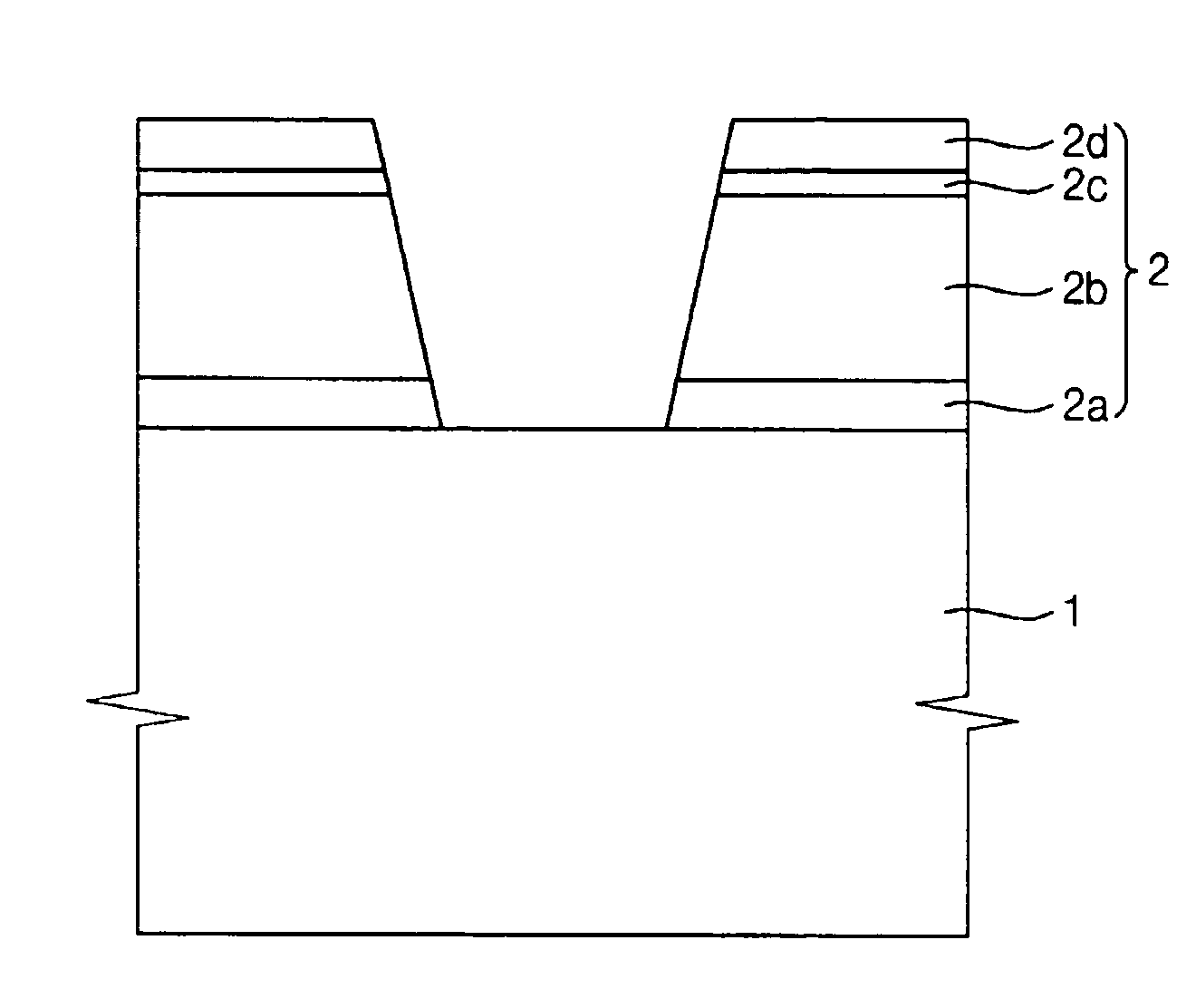
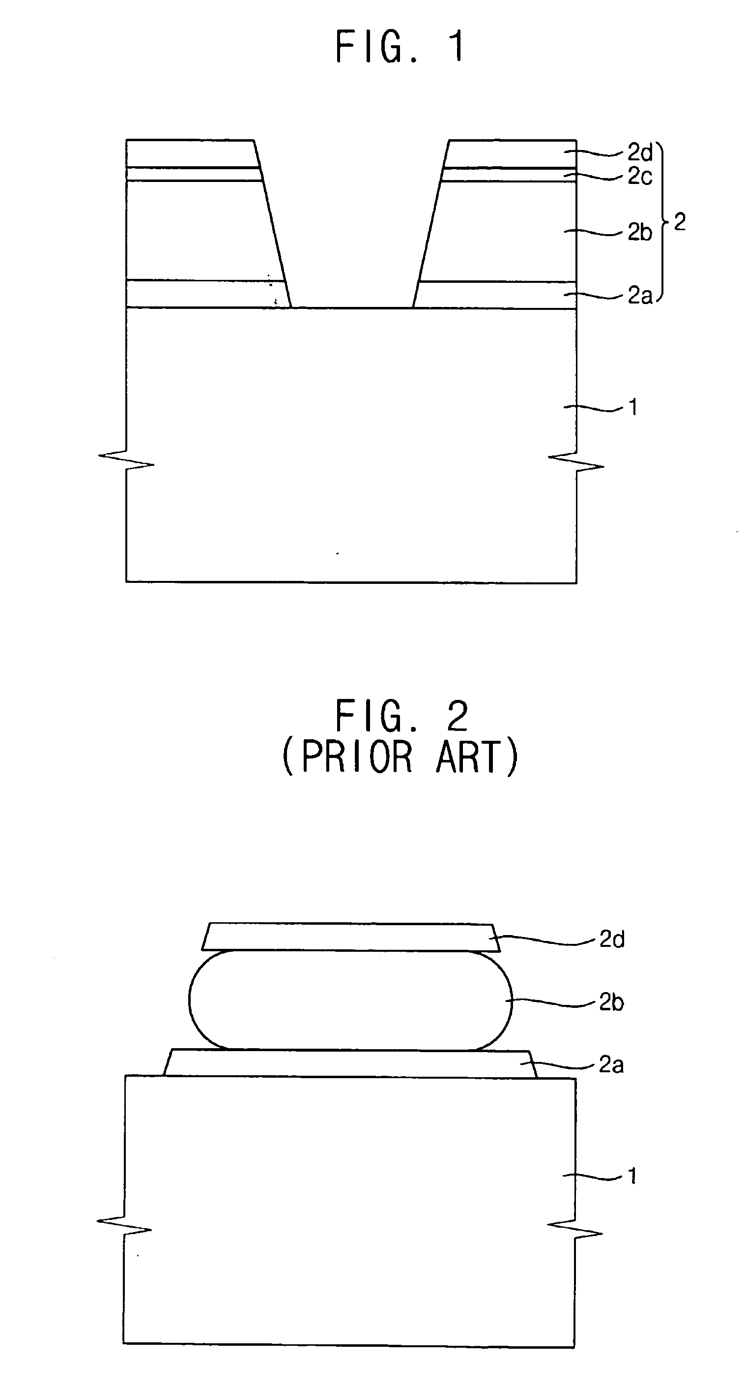
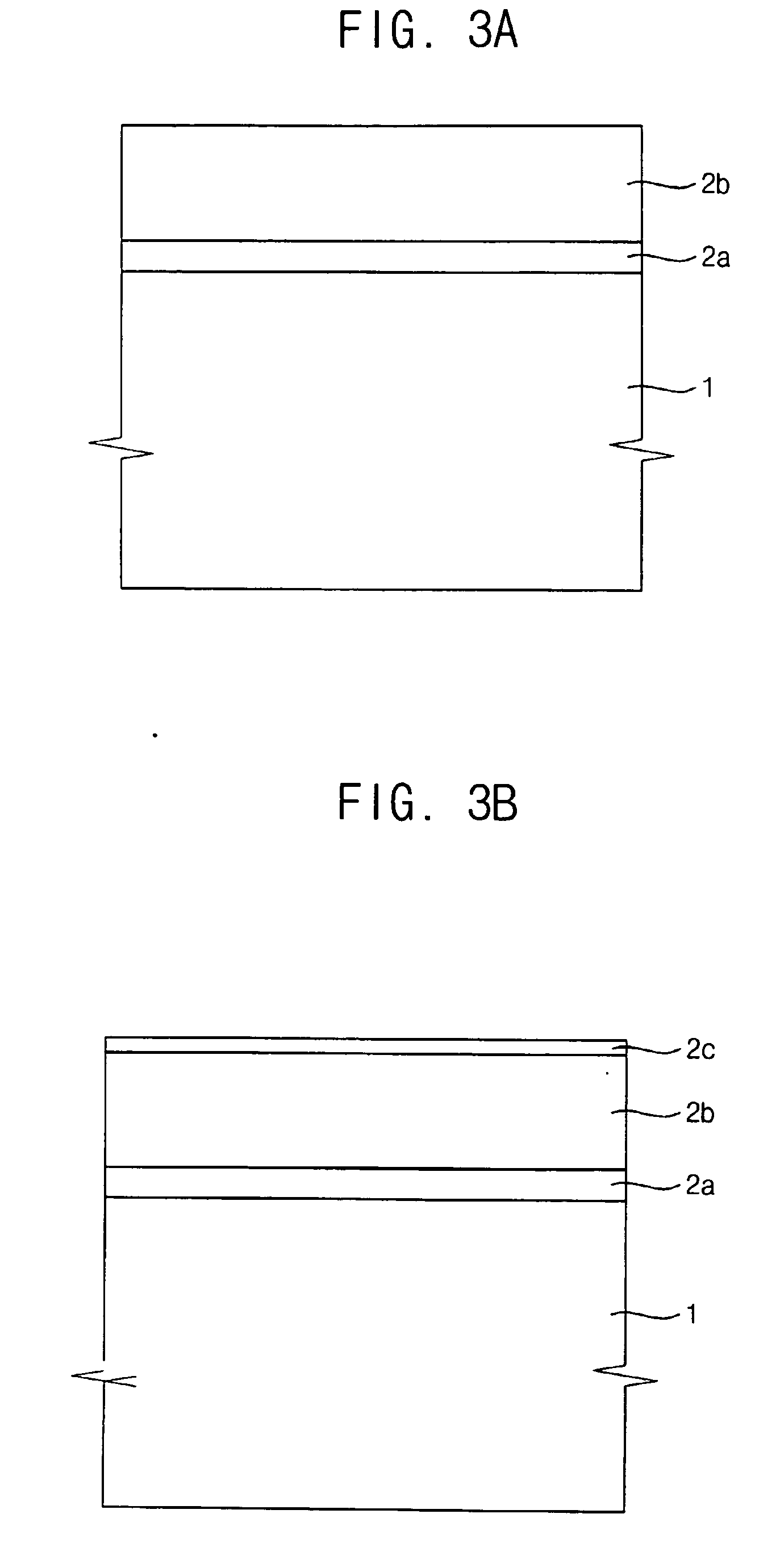
[0025] It will be understood that when an element or layer is referred to as being “on,”“connected to” or “coupled to” another element or layer, it can be directly on, connected or coupled to the other element or layer or intervening elements or layers may be present. In contrast, when an element is referred to as being “directly on,”“directly connected to” or “directly coupled to” another element or layer, there are no intervening elements or layers present. Like numbers refer to like elements throughout. As used herein, the singular forms “a,”“an” and “the” are intended to include the plural forms as well, unless the context clearly indicates otherwise. The regions illustrated in the figures are to be understood as being schematic in nature and variations from the shapes of the illustrations as a result, for example, of manufacturing techniques and / or tolerances, are to be expected. Thus, an implanted region illustrated as a rectangle will, typically, have rounded or curved featur...


PUM

PropertyMeasurementUnit
thicknessaaaaaaaaaa
thicknessaaaaaaaaaa
thicknessaaaaaaaaaa

Abstract

A conductive structure containing copper is capable of being etched to have a reliable profile where the copper layer is free of corrosion or oxidation includes a barrier layer formed on an insulating or semiconductor substrate followed by a copper layer, a blocking layer and a capping layer. The copper layer includes copper or copper alloy. The barrier layer includes molybdenum (Mo), molybdenum nitride (MoN) or molybdenum alloy which includes at least one of MoW, MoTi, MoNb or MoZr. The blocking layer includes copper nitride, copper oxide or copper oxinitride. The capping layer includes molybdenum, molybdenum nitride (MoN) or molybdenum alloy which includes at least one of MoW, MoTi, MoNb and MoZr.

Description

CROSS-REFERENCE TO RELATED APPLICATIONS [0001] This application relies for priority upon Korean Patent Application No. 2005-106274 filed on Nov. 8, 2005, the contents of which are herein incorporated by reference in its entirety. FIELD OF THE INVENTION [0002] The present invention relates to a conductive structure for use in a thin film transistor such as may be useful in the manufacture of liquid crystal and organic light-emitting displays and, more particularly, to a conductive structure that includes copper or copper alloy. DESCRIPTION OF THE RELATED ART [0003] A thin film transistor (TFT) substrate may be used in a liquid crystal display (LCD) or in an organic light-emitting device (OLED) display. An LCD includes two substrates having electrodes, and liquid crystal layer disposed therebetween. When electric fields are generated between the two electrodes, the arrangement of the liquid crystal molecules is changed, altering its optical transmissivity. An OLED displays an image by...

Claims


Application Information

Patent Timeline
Patent Type & Authority Applications(United States)
IPC IPC(8): B32B15/20B32B19/00C23C14/00B05D1/36
CPCG02F2001/13629G02F2001/136295Y10T428/12903H01L29/4908H01L27/124H01L29/458G02F1/13629G02F1/136295G02F1/136
Inventor LEE, JE-HUNKIM, SHI-YULKIM, DO-HYUNKIM, BYEONG-BEOMJEONG, CHANG-OHLEE, JUN-YOUNGBAE, YANG-HOKANG, SUNG-WOOK
Owner SAMSUNG ELECTRONICS CO LTD
Why Eureka
Try Eureka