Method for fabricating an NMOS transistor

Active Publication Date: 2007-05-31
UNITED MICROELECTRONICS CORP
View PDF13 Cites 11 Cited by
  • Summary
  • Abstract
  • Description
  • Claims
  • Application Information

AI Technical Summary

Benefits of technology

[0017] By conducting a carbon implantation process into the substrate and a corresponding amorphorized implantation process before or after the carbon implantation process is completed, the present invention eliminates the need of forming a recess for accommodating an epitaxial layer composed of silicon carbide while facilitates the formation of silicon carbide from the combination of both implantation processes. Preferably, by injecting atoms smaller than silicon into the sub

Problems solved by technology

However, if that same stress is applied to the conduction channel of an NMOS transistor, its drive current decreases.
However, as noted above, a pre-amorphorized implantation process is performed prior to the selective epitaxial growth by injecting atoms such as antimony or germanium into the silicon substrate for damaging the lattice structure of the substrate.
Since germanium or antimony used during the amorphorizing step

Method used


Image

  • Method for fabricating an NMOS transistor
  • Method for fabricating an NMOS transistor
  • Method for fabricating an NMOS transistor

Examples


Example

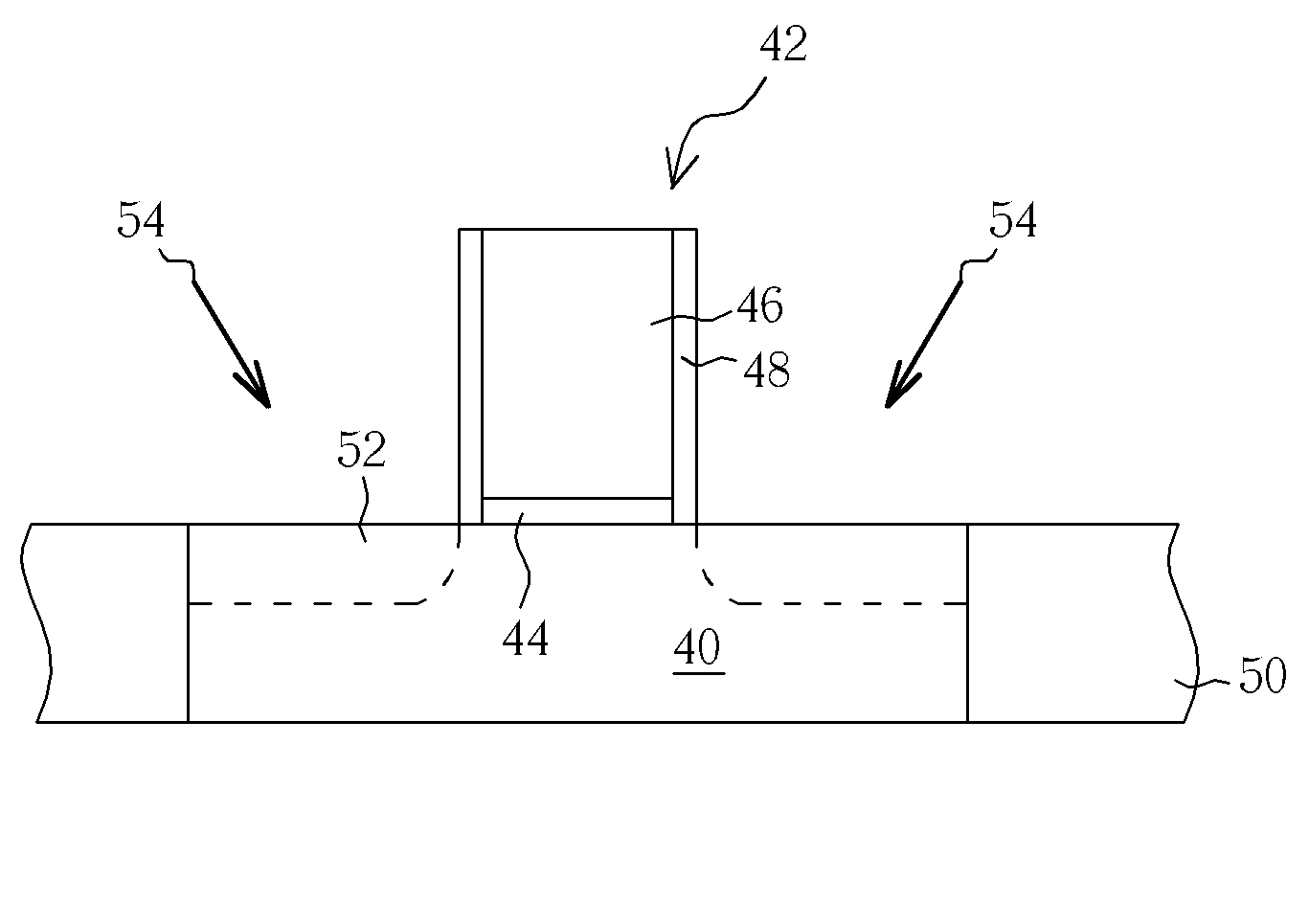
[0022] Please refer to FIGS. 6 through 11. FIGS. 6 through 11 illustrate a method for fabricating an NMOS transistor according to the present invention. As shown in FIG. 6, a substrate 40 having a gate structure 42 thereon is provided. The substrate 40 is preferably a wafer or a silicon on insulator (SOI) substrate, and the gate structure 42 is composed of a gate dielectric 44 and a gate 46. An offset spacer 48 is formed on the sidewall of the gate structure 42, and a shallow trench isolation 50 is formed surrounding the region outside the active area of the NMOS transistor.

[0023] As shown in FIG. 7, an amorphorized implantation process is performed with atoms smaller than silicon to disorder the polysilicon lattice of the substrate 40 for forming an amorphorized region 52 surrounding the gate structure 12. According to the preferred embodiment of the present invention, the implant species used for the amorphorized implantation may include any atom smaller than silicon, such as car...


PUM


Abstract

A method for fabricating an NMOS transistor is disclosed. First, a substrate having a gate structure thereon is provided. A carbon implantation process is performed thereafter by implanting carbon atoms into the substrate for forming a silicon carbide region in the substrate. Subsequently, a source/drain region is formed surrounding the gate structure. By conducting a carbon implantation process into the substrate and a corresponding amorphorized implantation process before or after the carbon implantation process is completed, the present invention eliminates the need of forming a recess for accommodating an epitaxial layer composed of silicon carbide while facilitates the formation of silicon carbide from the combination of both implantation processes.

Description

CROSS REFERENCE TO RELATED APPLICATIONS [0001] This application claims the benefit of the filing date of U.S. Provisional Patent Application No. 60 / 597,338, filed Nov. 25, 2005, the contents of which are hereby incorporated by reference.BACKGROUND OF THE INVENTION [0002] 1. Field of the Invention [0003] The invention relates to a method for fabricating an NMOS transistor. [0004] 2. Description of the Prior Art [0005] Both theoretical and empirical studies have demonstrated that carrier mobility in a transistor can be greatly increased when a stress of sufficient magnitude is applied to the conduction channel of a transistor to create a strain therein. Stress is defined as force per unit area. Strain is a dimensionless quantity defined as the change in a particular dimension of an item: for example, the change in the item's length, versus the initial dimension of that item: for example, its original length, when a force is applied in the direction of that dimension of the item: for e...

Claims


Application Information

Patent Timeline
IPC IPC(8): H01L21/336
CPCH01L21/26506H01L21/26513H01L29/165H01L29/6659H01L29/7848
Inventor HSIAO, TSAI-FUCHEN, PO-YUANCHEN, JUNG-CHIN
Owner UNITED MICROELECTRONICS CORP
Why Eureka
Try Eureka