Method for forming storage node contact plug in semiconductor device

a technology of contact plugs and semiconductor devices, which is applied in the direction of semiconductor devices, electrical equipment, basic electric elements, etc., can solve the problems of increasing maintenance costs, reducing the open area of the top part of each storage node contact plug, and reducing the overlay margin of storage nodes. , to achieve the effect of reducing manufacturing costs, reducing the generation of sac failure, and increasing the open area

Active Publication Date: 2007-05-31
SK HYNIX INC
View PDF2 Cites 39 Cited by
  • Summary
  • Abstract
  • Description
  • Claims
  • Application Information

AI Technical Summary

Benefits of technology

[0014] In one embodiment of the present invention relates to providing a method for forming a storage node contact plug in a semiconductor device, wherein the method can increase the open area at the top part of a storage node contact plug, reduce the generation of a SAC failure between a storage node and the storage node contact plug and reduce manufacturing costs using a cost-effective apparatus.

Problems solved by technology

However, since the storage node contact plugs are formed in the storage node contact holes, the open area at the top part of each of the storage node contact plugs is generally small.
Thus, the overlay margin for the storage nodes becomes too small, requiring the formation of a pad polysilicon layer between the storage node contact plugs and the storage nodes.
For this process, an expensive etching apparatus is generally used increasing the maintenance cost, thereby impeding mass production.
The damage to the bit line hard mask layer may cause SAC failures such as a short circuit between the storage nodes and the storage node contact plugs.

Method used


Image

  • Method for forming storage node contact plug in semiconductor device
  • Method for forming storage node contact plug in semiconductor device
  • Method for forming storage node contact plug in semiconductor device

Examples


Embodiment Construction

[0030] Hereinafter, various embodiments of the present invention will be described in detail with reference to the accompanying drawings.

[0031]FIG. 4 is a top view of a semiconductor device in accordance with an embodiment of the present invention.

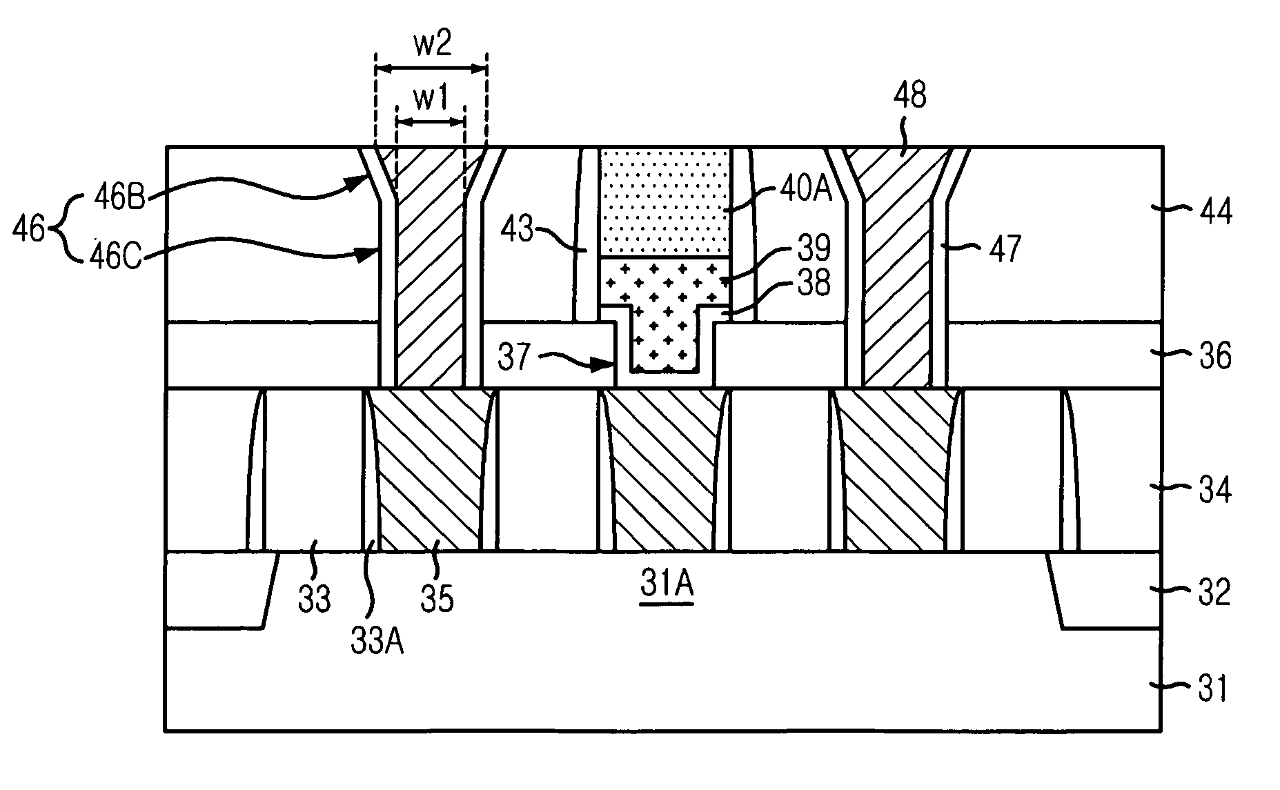
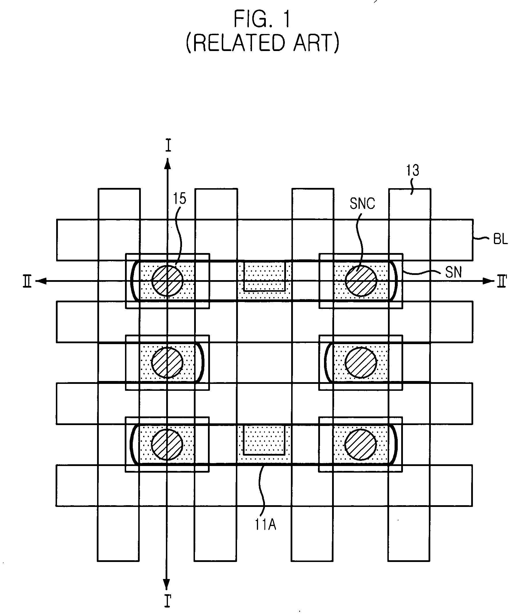
[0032] As illustrated, a plurality of gate lines 33 are arranged over active regions 31A. A plurality of landing plug contacts 35 are formed over the active regions 31A disposed between the gate lines 33 and a plurality of bit lines BL arranged perpendicular to the gate lines 33 to be coupled with a group of the landing plug contacts 35.

[0033] A plurality of storage node contact plugs 48 are formed over the landing plug contacts 35 in a region where the gate lines 33 and the bit lines BL cross each other. A plurality of storage nodes SN are formed over the storage node contact plugs 48.

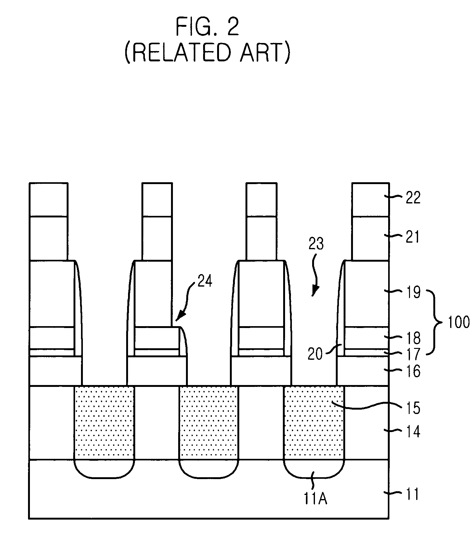
[0034] Although not illustrated, using line type storage node contact masks, storage node contact holes are created where the storage node contact plugs...


PUM


Abstract

A method for forming a storage node contact plug in a semiconductor device is provided. The method includes: forming an inter-layer insulation layer over a substrate having a conductive plug; etching a portion of the inter-layer insulation layer using at least line type storage node contact masks as an etch mask to form a first contact hole with sloping sidewalls; etching another portion of the inter-layer insulation layer underneath the first contact hole to form a second contact hole exposing the conductive plug, the second contact hole having substantially vertical sidewalls; and filling the first and second storage node contact holes to form a storage node contact plug.

Description

BACKGROUND OF THE INVENTION [0001] The present invention relates to a method for fabricating a semiconductor device; and more particularly, to a method for forming a storage node contact plug in a semiconductor device. [0002] In storage node contact plugs with a feature size of less than 80 nm, the large scale of integration in semiconductor devices have led to formation of hole type contacts using ArF photoresist. [0003]FIG. 1 is a top view illustrating a typical semiconductor device. [0004] A plurality of gate lines 13 are arranged on active regions 11A in one direction. A plurality of landing plug contacts 15 are formed on the respective active regions 11A between the gate lines 13. A plurality of bit lines BL are arranged perpendicular to the gate lines 13 to be connected with a group of the landing plug contacts 15. A plurality of storage node contact plugs SNC are formed on the landing plug contacts 15 in a region where the bit lines BL and the gate lines 13 cross with each ot...

Claims


Application Information

Patent Timeline
Patent Type & Authority Applications(United States)
IPC IPC(8): H01L21/44
CPCH01L21/76804H01L21/76831H01L21/76897H01L27/10855H10B12/0335H01L21/28
Inventor HWANG, CHANG-YOUNKIM, HYUNG-HWANCHOI, IK-SOOLEE, HAE-JUNG
Owner SK HYNIX INC
Why Eureka
Try Eureka