
Short and thin silicon cantilever with tip and fabrication thereof

a silicon cantilever and tip technology, applied in the field of scanning probe microscopy, can solve the problems of difficult thin fabrication, extremely difficult to prepare cantilevers thinner than 1 m in a wafer scale by this process

Active Publication Date: 2007-06-07
UNIV HOUSTON SYST
View PDF13 Cites 2 Cited by
  • Summary
  • Abstract
  • Description
  • Claims
  • Application Information

AI Technical Summary

Benefits of technology

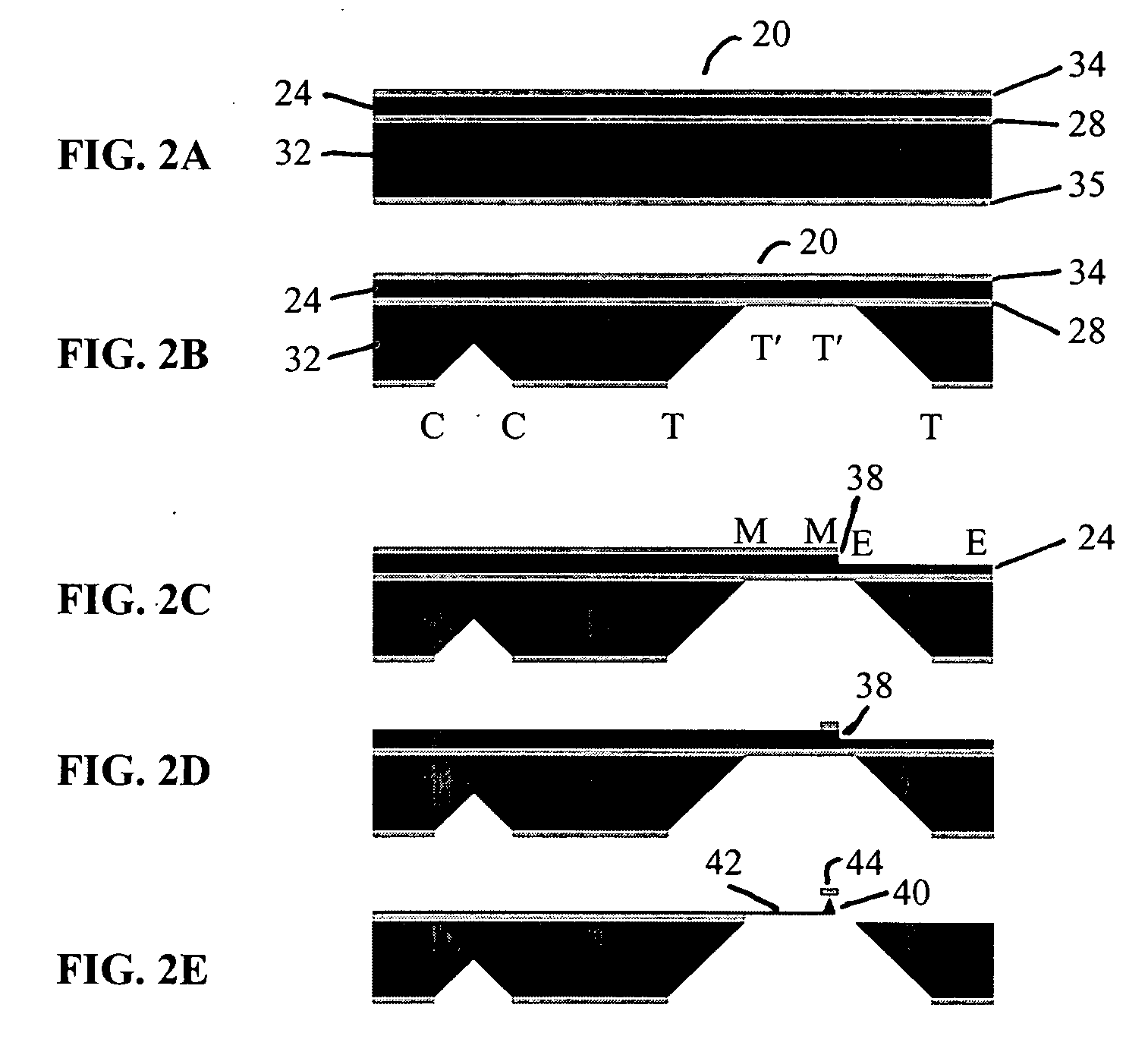
[0007] Thin and short cantilevers possess both a low force constant and a high resonance frequency, which are highly desirable for atomic force microscope (AFM) imaging and force measurement. According to some embodiments, the present invention provides small silicon (Si) cantilevers integrated with Si tips, for example fabricated from SOI wafers. SOI wafers are used to reduce the variation of the cantilevers' thickness. In one example, the fabrication process provided SOI chips containing 40 silicon cantilevers integrating with an ultra-sharp Si tip. These tips produced images having a much higher resolution than the resolution produced by commercial tips. Also, these tips had a much lower force constant, which is more suitable for imaging soft samples, than those of commercial tips. The availability of such SOI chips greatly facilitates large scale modification of the silicon cantilever tips' surfaces. These tips can be modified with a monolayer of oligo (ethylene glycol) derivatives (see U.S. patent application Ser. No.10 / 742,047) that resist the non-specific interactions with proteins, rendering them most suitable for imaging and measurement of biological samples.

Problems solved by technology

This situation reflects the difficulties of fabricating thin Si cantilever tips.
Due to the deviation of thickness over the whole wafer, and the difficulties in controlling the etching process, it is extremely difficult to prepare cantilevers thinner than 1 μm in a wafer scale by this process.
However, to take advantage of such micron-sized cantilevers requires specially designed AFM heads that remain at the prototyping stage and are available in only a few research groups.

Method used


Image

  • Short and thin silicon cantilever with tip and fabrication thereof
  • Short and thin silicon cantilever with tip and fabrication thereof
  • Short and thin silicon cantilever with tip and fabrication thereof

Examples


Embodiment Construction

[0022] The following discussion is presented to enable a person skilled in the art to make and use the invention. The general principles described herein may be applied to embodiments and applications other than those detailed below without departing from the spirit and scope of the present invention as defined by the appended claims. The present invention is not intended to be limited to the embodiments shown, but is to be accorded the widest scope consistent with the principles and features disclosed herein.

[0023] As such, those skilled in the art will appreciate that the conception, upon which this disclosure is based, may readily be utilized as a basis for the designing of other structures, methods, and devices for carrying out the several purposes of the present invention. It is important, therefore, that the claims be regarded as including such equivalent constructions insofar as they do not depart from the spirit and scope of the present invention.

Design:

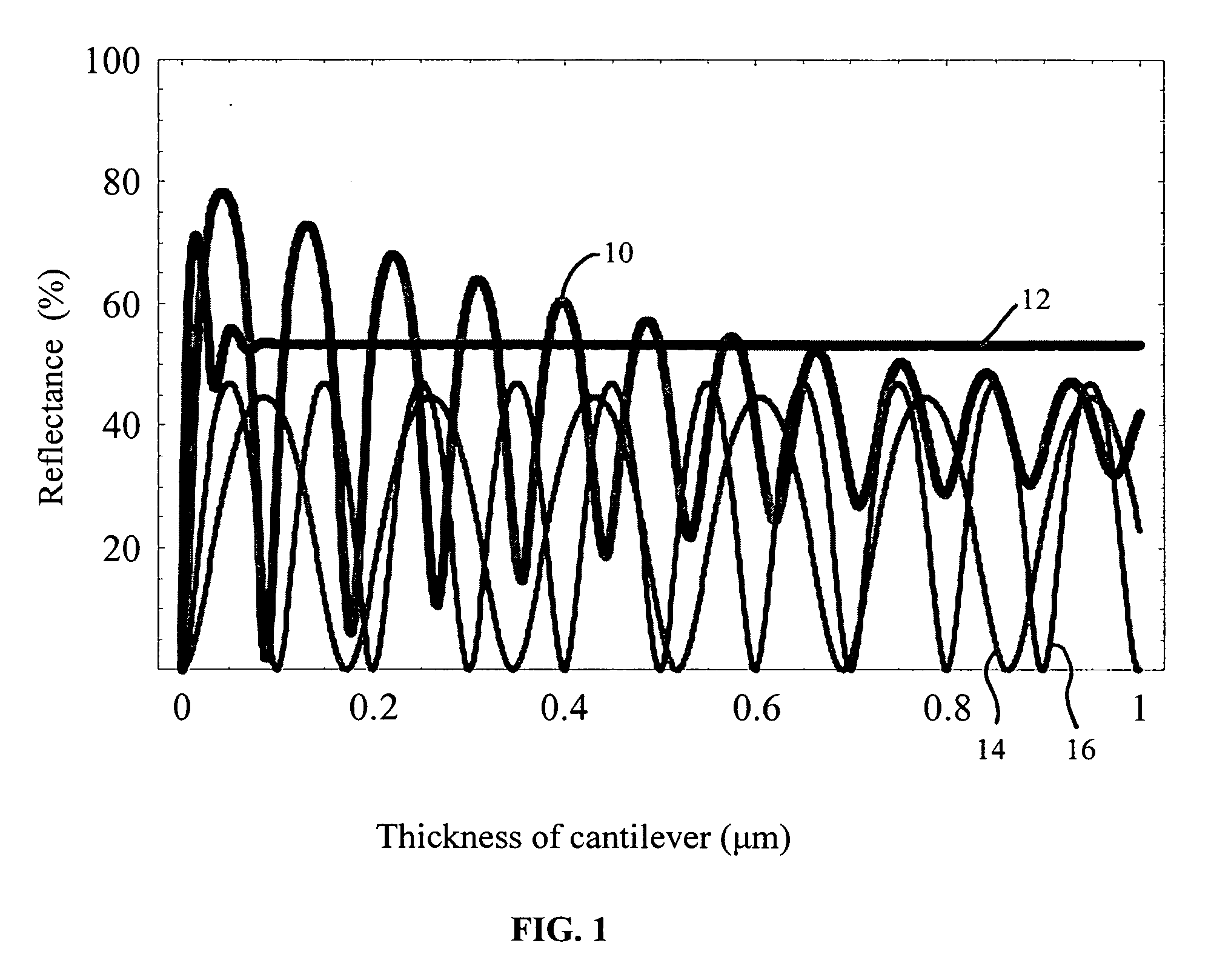
[0024] The thin f...


PUM

PropertyMeasurementUnit
heightaaaaaaaaaa
heightaaaaaaaaaa
sizeaaaaaaaaaa

Abstract

Thin and short cantilevers possess both a low force constant and a high resonance frequency, thus are highly desirable for atomic force microscope (AFM) imaging and force measurement. According to some embodiments, the invention provides small silicon (Si) cantilevers integrated with a Si tip, for example fabricated from SOI wafers that are used for reducing the variation of thickness of the cantilevers. In one example, the fabrication process provided SOI chips containing 40 silicon cantilevers integrating with an ultra-sharp Si tip. The resolution of images obtained with these tips was much higher than those obtained with the commercial tips, while the force constants were much less, that is, more suitable for imaging soft samples. The availability of such SOI chips greatly facilitates large scale modification of the surfaces of the silicon cantilever tips with a monolayer of oligo(ethylene glycol) derivatives that resist the non-specific interactions with proteins, rendering them most suitable for imaging and measurement of biological samples.

Description

CROSS-REFERENCES TO RELATED APPLICATIONS [0001] This application claims the benefit of U.S. Provisional Application No. 60 / 736,924, filed Nov. 15, 2005. The present application is related to U.S. application Ser. No. 10 / 742,047, filed on Dec. 19, 2003, and published on Oct. 28, 2004. U.S. application Ser. No. 10 / 742,047 is hereby incorporated herein by reference.FEDERAL SPONSORSHIP [0002] This invention was made in part with United States Government support under a National Science Foundation grant CTS-0210840. The U.S. Government has certain rights in this invention.FIELD OF THE INVENTION [0003] This invention generally relates to the field of scanning probe microscopy, and more particularly relates a silicon cantilever with tip and a method of fabricating same. BACKGROUND [0004] Recently, short and thin cantilevers have been used for atomic force microscope (AFM) imaging and force measurement [D. A. Walters, J. P. Cleveland, N. H. Thomson, P. K. Hansma, M. A. Wendman, G. Gurley, V...

Claims


Application Information

Patent Timeline
Patent Type & Authority Applications(United States)
IPC IPC(8): G12B21/08H01L21/302G01Q60/38G01Q10/00G01Q60/24G01Q70/14G01Q70/16
CPCB82Y35/00Y10S977/879Y10S977/863G01Q60/38
Inventor CAI, CHENGZHIYAM, CHIN-MINGQIN, GUOTINGPEI, STEVENYU, QINGKAI
Owner UNIV HOUSTON SYST
Learn More