Solid-state image pickup apparatus
a solid-state image and pickup technology, applied in the field of solid-state image pickup apparatus, can solve the problems of lateral stripe on the image screen, difficult to supply an exact black reference signal, and adverse effects
- Summary
- Abstract
- Description
- Claims
- Application Information
AI Technical Summary
Problems solved by technology
Method used
Image
Examples
first embodiment
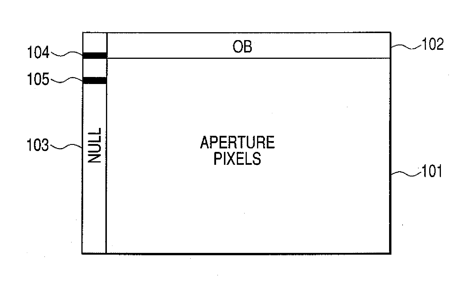
[0027]FIG. 1 is a plan view showing an example of the configuration of a solid-state image pickup apparatus according to a first embodiment of the present invention. As shown in FIG. 1, the solid-state image pickup apparatus of this embodiment includes a photoelectric conversion signal outputting region 101, a first black reference signal outputting region 102, and a second black reference signal outputting region 103.
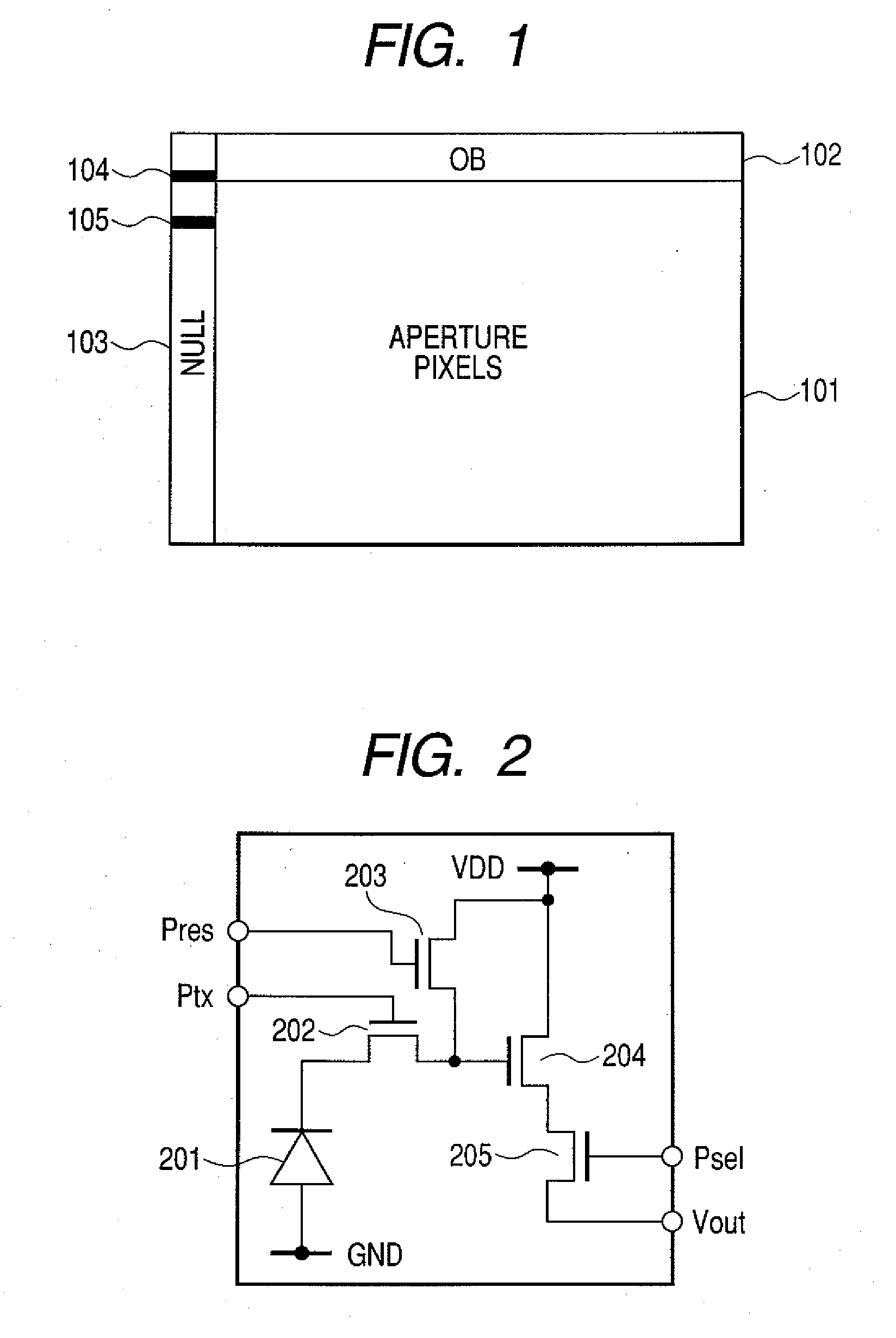
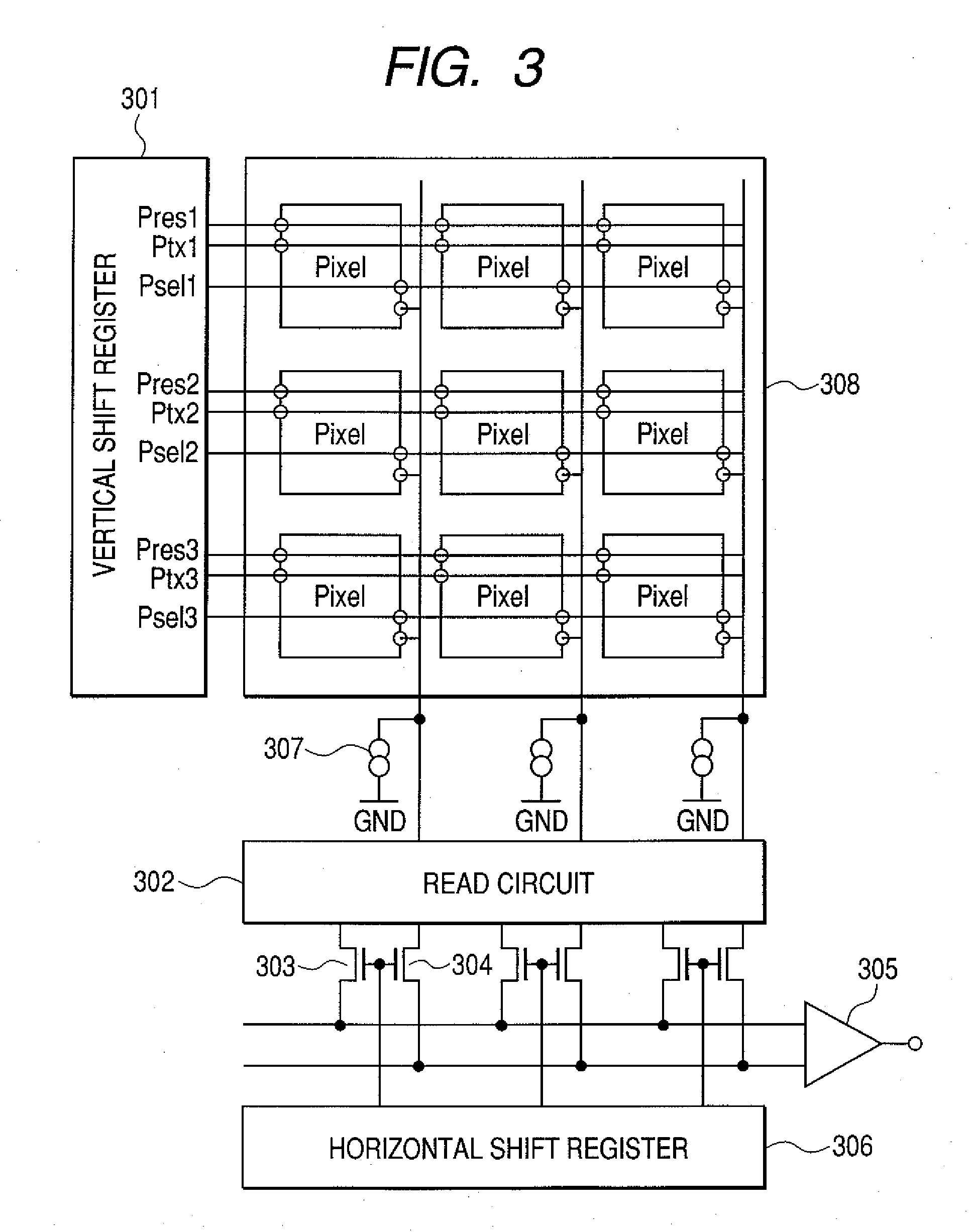
[0028] In the photoelectric conversion signal outputting region 101, a large number of photoelectric conversion signal outputting elements are arranged. The photoelectric conversion signal outputting elements can also be called pixels, and composed of a photoelectric conversion device such as a photo-diode, and a reading circuit for reading the signal of the photoelectric conversion device.
[0029] The first black reference signal outputting region 102 is a light shielded region provided neighboring the photoelectric conversion signal outputting region 101 in the verti...
second embodiment
[0050]FIG. 10 is a block diagram showing an example of a configuration of a reading circuit 302 of a second embodiment of the present invention. The difference from the general reading circuit in FIG. 4 is in that the reading circuit 302 has two lines of the reference voltage of the clamping circuit and configured so that the reference voltages VCOR1 and VCOR2 are supplied by clamping voltage selection signals Pvsel1 and Pvsel2 . According to this configuration, only when the second black reference signal outputting region 103 is clamped, it is possible to shift the level of the signal outputted from the output terminal OUT by the operations shown below.
[0051] A clamping voltage selection signal Pvres1 is made to be high-level and in an activated state, a clamping voltage selection signal Pvsel2 is made to be low-level and in an inactivated state, and a signal to be supplied to the gate line PcOr of a clamping switch is made to be high-level and in activated state. After that, the ...
third embodiment
[0054]FIG. 11 shows the block diagram of the signal-processing circuit unit of an image pickup system using a solid-state image pickup device according to a third embodiment of the present invention. The sensor signal outputted from the solid-state image pickup apparatus is amplified at a programmable gain amplifier (PGA) 1001. At that time, the reference signal is supplied by converting the digital signal generated by an OB clamping block 1005 into an analog signal using a digital-to-analog converter (DAC) 1006. An analog-to-digital converter (ADC) 1002 converts the output signals of the programmable gain amplifier 1001 as analog signals into digital signals. A register 1003 averages the output signals from the second black reference signal outputting region 103, and memorizes the averaged signal value. A subtracter 1004 subtracts the average value of the register 1003 from the output signals of the analog-to-digital converter 1002, and outputs a signal. The signal from the subtrac...
PUM
 Abstract
Description
Claims
Application Information


