Semiconductor integrated circuit device and IC card equipped with the same

a technology of integrated circuits and semiconductors, applied in the direction of relays, error detection/correction, instruments, etc., can solve the problems of insufficient voltage supply of internal power supply lines, inability to thoroughly disconnect internal power supply lines from contact power supply terminals, and inability to supply internal power supply lines with sufficient voltage, etc., to reduce the on-resistance of mos transistors, reduce the time interval needed to start operating chips, and reduce the effect of mos transistor siz

Active Publication Date: 2007-06-07
RENESAS ELECTRONICS CORP
View PDF4 Cites 36 Cited by
  • Summary
  • Abstract
  • Description
  • Claims
  • Application Information

AI Technical Summary

Benefits of technology

[0014] It is a second object associated with the first object of the present invention to provide a circuit technology capable of decreasing an on-resistance of an MOS transistor constituting a power supply switch circuit without increasing the MOS transistor size.
[0015] It is a third object associated with the second object of the present invention to provide a circuit technology capable of minimizing a time interval needed to start operating a chip.

Problems solved by technology

The internal power supply line cannot be thoroughly disconnected from the contact power supply terminal.
When the power supply switch circuit uses an NMOS transistor, decreasing a power supply voltage supplied from the contact power supply terminal requires a long time to generate a gate voltage large enough to turn on the NMOS transistor.
In the meantime, the internal power supply line is not supplied with a sufficient voltage.
It becomes difficult to perform the other processes such as operation mode judgment, and a certain amount of time was needed until start of operation of a chip.

Method used


Image

  • Semiconductor integrated circuit device and IC card equipped with the same
  • Semiconductor integrated circuit device and IC card equipped with the same
  • Semiconductor integrated circuit device and IC card equipped with the same

Examples


Embodiment Construction

[0034] The following describes in more detail the semiconductor integrated circuit device and the IC card according to the invention with reference to an embodiment shown in the accompanying drawings.

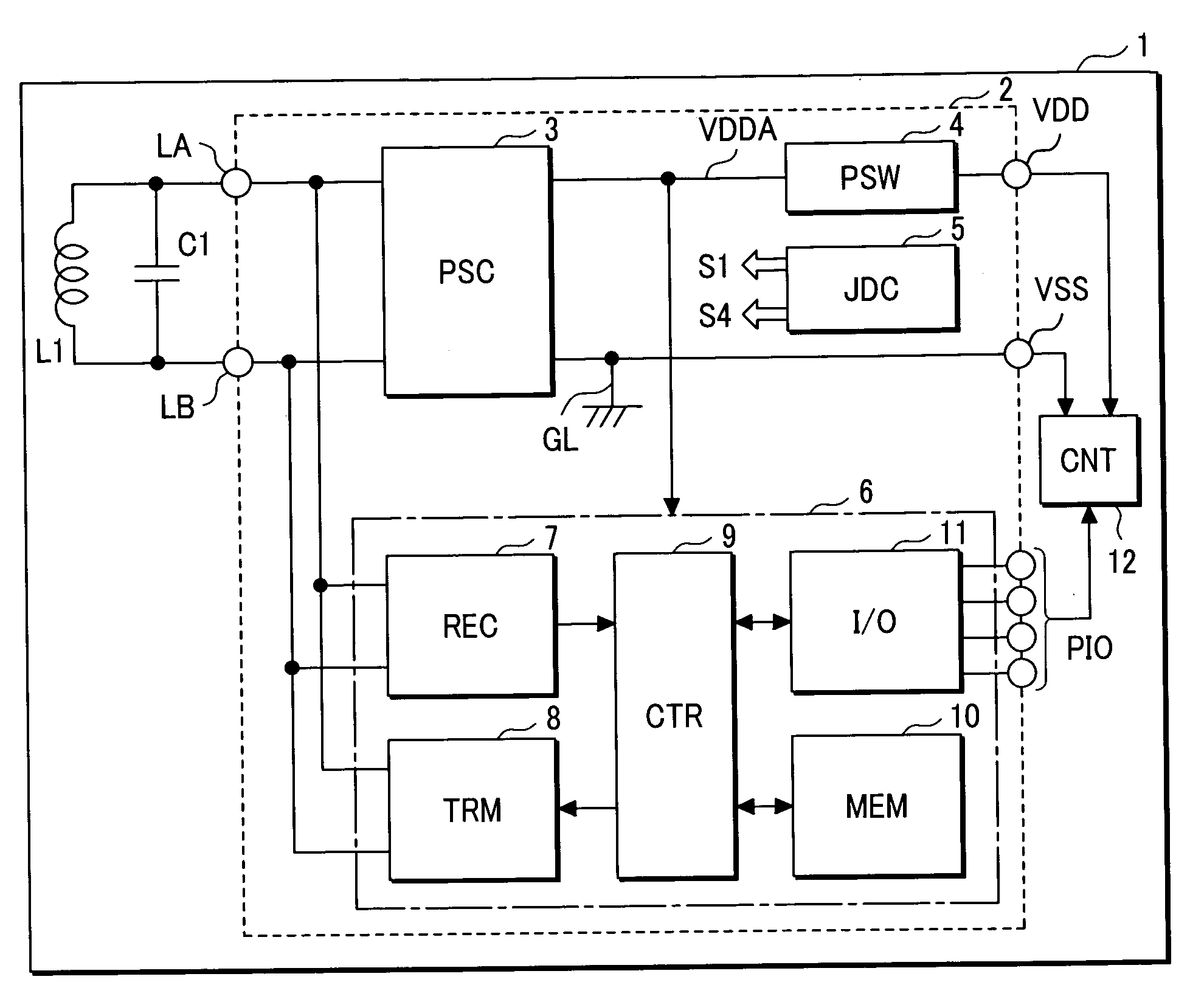
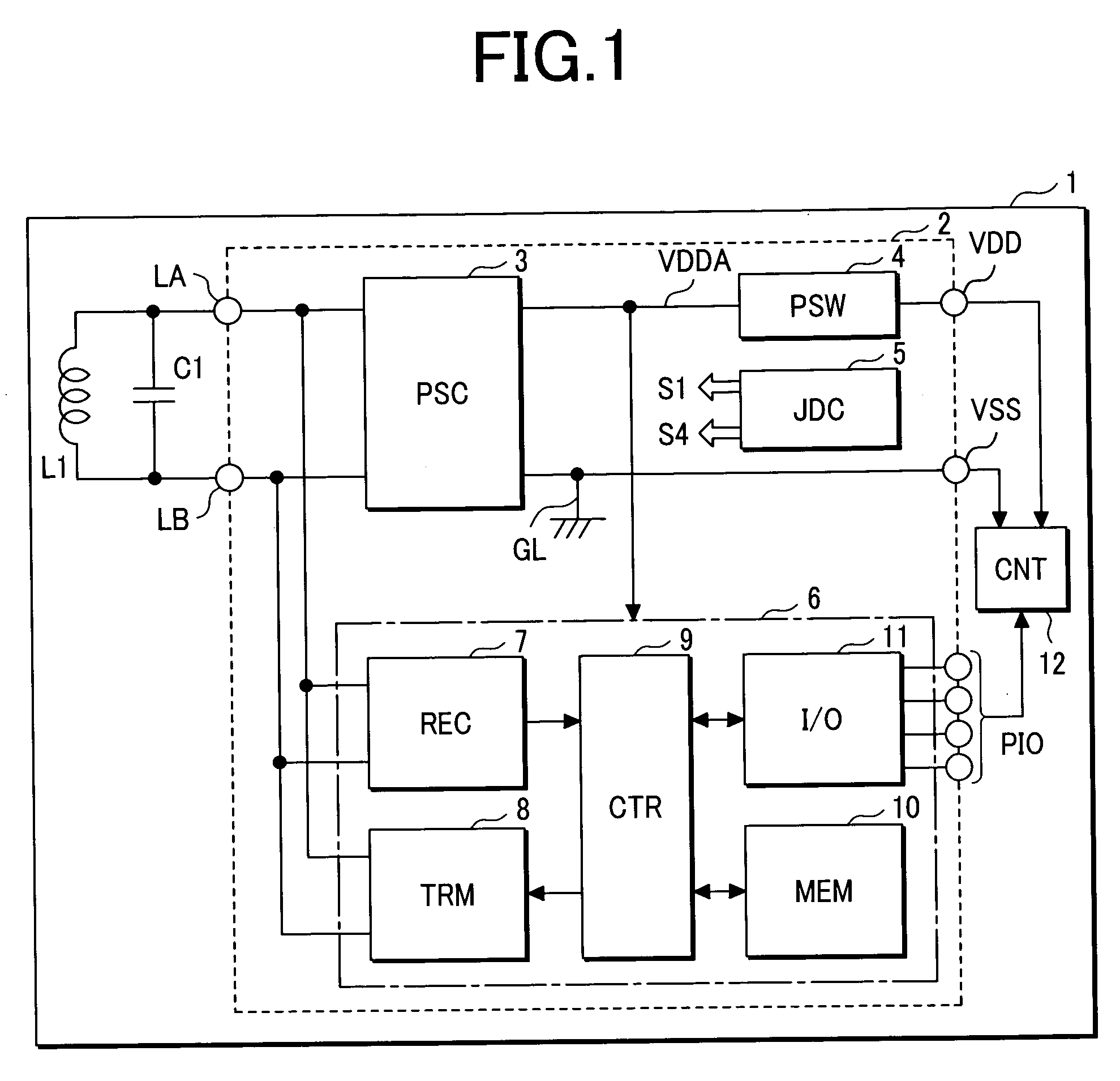
[0035]FIG. 1 is a basic construction diagram illustrating an embodiment of the semiconductor integrated circuit device and the IC card according to the invention.

[0036] In FIG. 1, reference numeral 1 denotes an IC card; 2 denotes a semiconductor integrated circuit device mounted on the IC card 1; and L1 denotes an antenna mounted on the IC card 1. A capacitor CA connected to the antenna L1 constructs a resonance circuit. The resonance capacitor CA is adjusted in consideration for a parasitic capacitor or the like and need not be always connected. The semiconductor integrated circuit device 2 includes a power supply circuit (PSC) 3, a power supply switch circuit (PSW) 4, a contact / contactless judgment circuit (JDC) 5, and an internal circuit 6. The semiconductor integrated circuit devi...


PUM


Abstract

There is a need for turning off a transistor in a power supply switch circuit irrespective of relative potential relationship between a contact power supply terminal and an internal power supply line and making it possible to decrease an on-resistance of an MOS transistor without increasing the size of the MOS transistor constituting the power supply switch circuit. The power supply switch circuit is comprised of two PMOS transistors whose gate terminals connect with two pull-up circuits. A charge pump circuit generates a negative voltage and is connected to a pull-down circuit. The pull-down circuit is connected to the gate terminals in common. During a contactless operation, the pull-up circuit short-circuits one gate terminal to a contact power supply terminal VDD and the other gate terminal to an internal power supply line VDDA. During a contact operation, the pull-up circuit supplies both gate terminals with a negative voltage from the charge pump circuit.

Description

CLAIM OF PRIORITY [0001] The present patent application claims priority from Japanese application JP No. 2005-350133 filed on Dec. 5, 2005, the content of which is hereby incorporated by reference into this application. FIELD OF THE INVENTION [0002] The present invention relates to a power supply control technology appropriately applied to a semiconductor integrated circuit device and the like mounted on an IC card. More specifically, the invention relates to a semiconductor integrated circuit device and an IC card using the same that operate selectively on a power supply voltage generated from an electromagnetic wave received at an antenna provided for the IC card and a power supply voltage supplied from the outside via a contact terminal provided for the IC card. BACKGROUND OF THE INVENTION [0003] There is an IC card that can function both as a contact IC card and a contactless IC card. When the IC card is used as a contact IC card, it uses a power supply voltage supplied from an ...

Claims


Application Information

Patent Timeline
Patent Type & Authority Applications(United States)
IPC IPC(8): H01H47/00G06K19/07
CPCG06K19/0701G06K19/0723
Inventor WATANABE, KAZUKI
Owner RENESAS ELECTRONICS CORP
Why Eureka
Try Eureka