Shift register

a technology of shift register and shift register, which is applied in the field of shift register, can solve the problems of sup>th /sup>transistor suffering from aging, and achieve the effect of minimizing bias stress

Active Publication Date: 2007-06-07
LG DISPLAY CO LTD
View PDF4 Cites 37 Cited by
  • Summary
  • Abstract
  • Description
  • Claims
  • Application Information

AI Technical Summary

Benefits of technology

[0059] An object of the present invention is to provide a shift register minimizing bias stress applied to a transistor.

Problems solved by technology

Although the conventional bi-direction shift register is operated such that the 9th transistor can input a successive high voltage to its gate as the voltage of the third node Q3 is maintained at a low level during the intervals t1 and t2 and kept at a high state during the other intervals, it has disadvantages in that the 9th transistor suffers from aging due to bias stress caused by a voltage with a high level applied to the gate, in which the high voltage is provided to the third node Q3.

Method used


Image

  • Shift register
  • Shift register
  • Shift register

Examples


Embodiment Construction

[0073] Reference will now be made in detail to the preferred embodiments of the present invention, examples of which are illustrated in the accompanying drawings. Wherever possible, the same reference numbers will be used throughout the drawings to refer to the same or like parts.

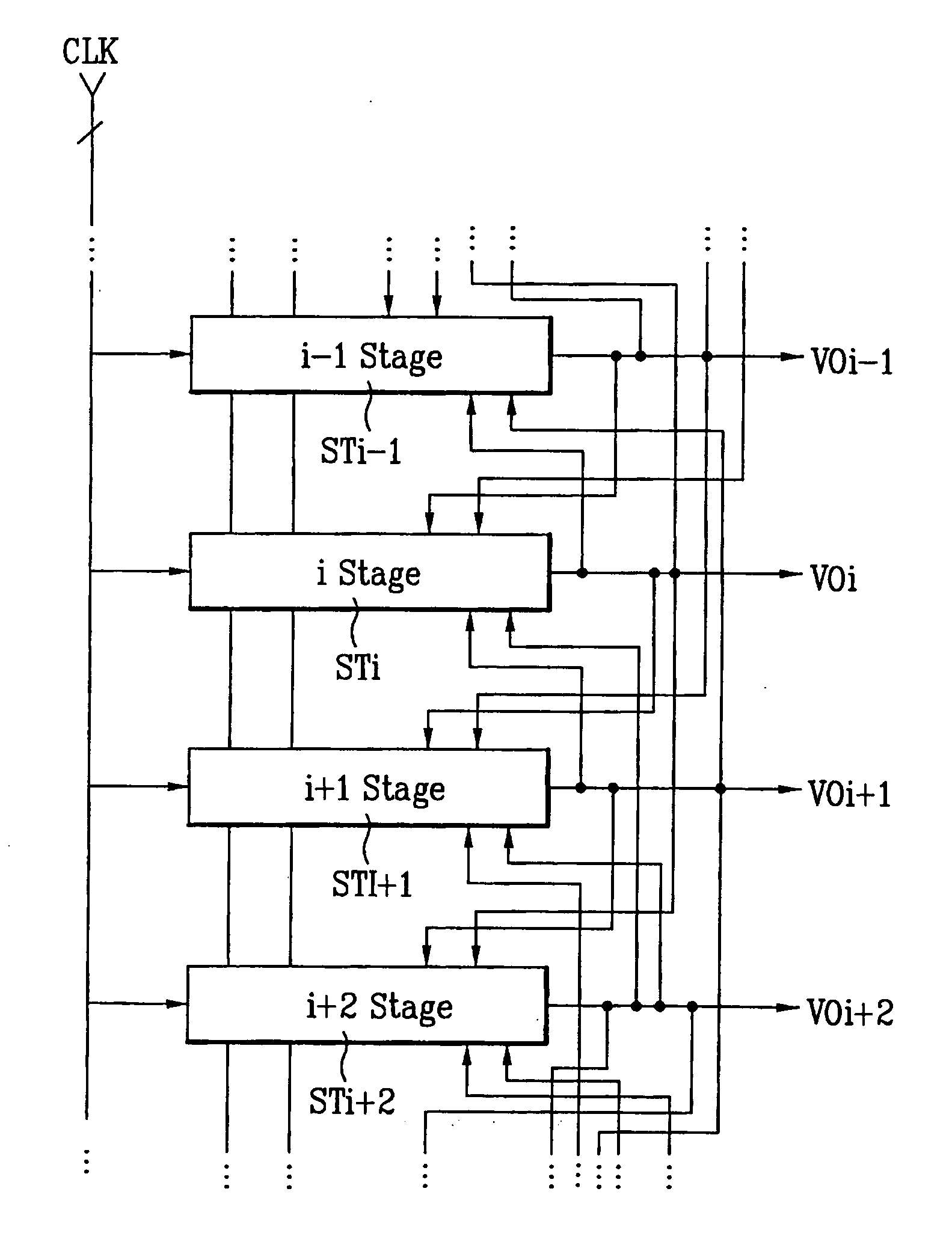
[0074]FIG. 5 illustrates a schematic block diagram of the shift register according to an embodiment of the present invention.

[0075] Referring to FIG. 5, the shift register according to the present invention includes n stages, ST1-STn that are dependently connected to first and second clock pulse providing lines, first and second voltage providing lines, a drive voltage line and a ground voltage line. Here, first voltage Vd1 and second voltage Vd2, which are provided to the first and second voltage providing lines, respectively, have opposite phases to one another according to scan direction. First and second clock signals CLK are provided to the first and second clock pulse providing lines, respectively, ...


PUM


Abstract

A shift register minimizing bias stress applied to transistors is disclosed. A shift register including n stages outputting scan pluses that are sequentially delayed in a forward or reverse direction thereof, where n is positive integer and wherein each stage includes: a scan direction controller that provides a first or second voltage to a scan direction control node according to a first or second enable signal and controlling the forward or reverse direction output; a first node controller that controls a first node according to a voltage on the scan direction control node; a second node controller that controls a second node according to the voltage on the scan direction control node and a voltage on the first node; an output unit that outputs a clock signal as scan pulse according to voltages on the first and second nodes; a third node controller that provides one of the first and second voltages to a third node according to the first and second enable signals; a first discharge circuit unit that discharges the voltage on the first node according to voltages of the second and third nodes; and a second discharge circuit unit that discharges the voltage on the third node according to one of a third enable signal and a fourth enable signal.

Description

[0001] This application claims the benefit of the Korean Patent Application No. 10-2005-116838, filed on Dec. 2, 2005, which is hereby incorporated by reference as if fully set forth herein.BACKGROUND OF THE INVENTION [0002] 1. Field of the Invention [0003] The present invention relates to a shift register, and more particularly, to a shift register minimizing a bias stress applied to a switching element. [0004] 2. Discussion of the Related Art [0005] Recently, various flat-panel display devices have appeared on the market to overcome the disadvantages of a cathode ray tube (CRT), such as, weight, volume, etc. Such flat-panel display devices include a liquid crystal display (LCD), a field emission display (FED), a plasma display panel (PDP), a light emitting display (LED), etc. [0006] A conventional LCD displays images thereon as the light transmission of a liquid crystal layer is controlled using electric fields. To this end, the LCD includes an LCD panel in which liquid crystal (L...

Claims


Application Information

Patent Timeline
Patent Type & Authority Applications(United States)
IPC IPC(8): G11C19/00
CPCG11C19/28G09G3/36G02F1/133H03K23/44
Inventor MOON, SU HWANKIM, DO HEONCHAE, JI EUN
Owner LG DISPLAY CO LTD
Why Eureka
Try Eureka