Interconnect structure of an integrated circuit and manufacturing method thereof

a technology of interconnection structure and manufacturing method, which is applied in the manufacture of printed circuits, printed circuit aspects, basic electric elements, etc., can solve the problems of not meeting the requirements, unable to provide flexibility, and a lot of process problems, so as to achieve the effect of strong contact strength and high density of hooks

Active Publication Date: 2007-06-07
IND TECH RES INST
View PDF5 Cites 11 Cited by
  • Summary
  • Abstract
  • Description
  • Claims
  • Application Information

AI Technical Summary

Benefits of technology

[0011] In addition to achieving the property of flexibility, the special contact design can absorb the stress resulting from thermal or flexible deformation. In the structure, a plurality of tiny pillars made of conductive materials is formed on the both sides of the contact surface. With the different densities and thicknesses of the pillars on both sides, a tight connecting can be achieved due to the contact strength generated when both side

Problems solved by technology

However, in recent research of flexible electronic packaging, there is no solution that meets the requirement of flexibility directed to the interconnection between individual devices.
The process is rather bothersome and cannot provide flexibility, and the contacts cannot b

Method used


Image

  • Interconnect structure of an integrated circuit and manufacturing method thereof
  • Interconnect structure of an integrated circuit and manufacturing method thereof
  • Interconnect structure of an integrated circuit and manufacturing method thereof

Examples


first embodiment

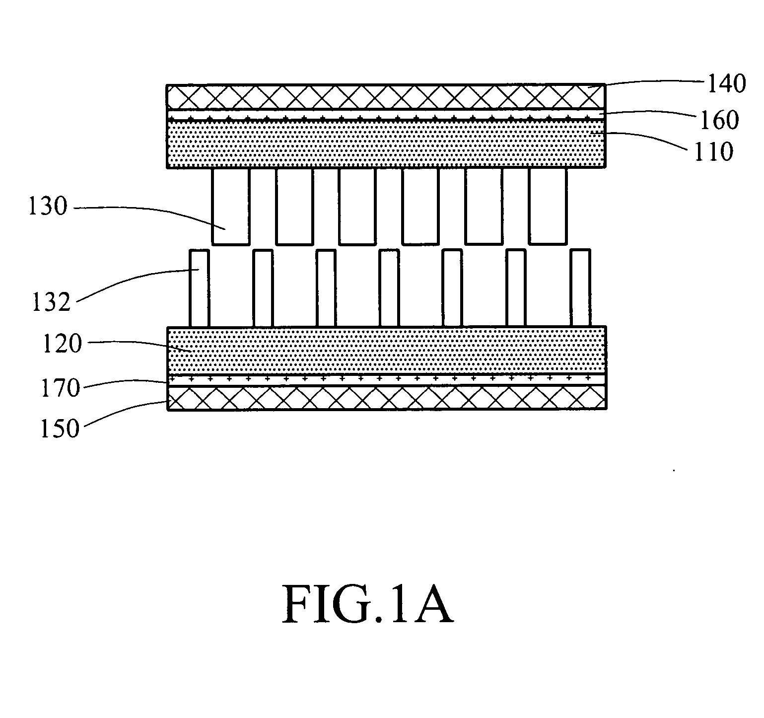
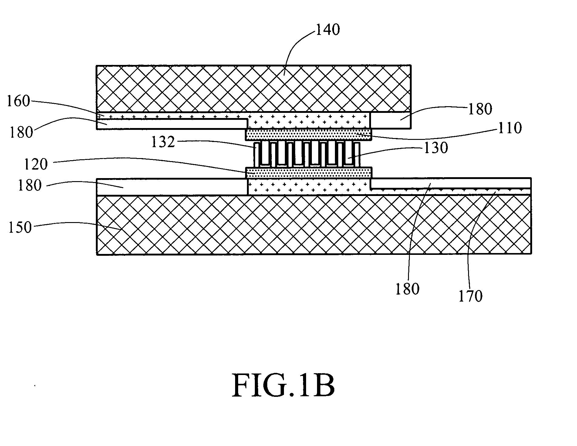
[0024] Referring to FIG. 1A, it shows a schematic view of an interconnect structure of an integrated circuit according to the present invention for interconnecting a first substrate 140 and a second substrate 150. The interconnect structure comprises a first pad 110, a plurality of first pillars 130, a second pad 120, and a plurality of second pillars 132, which are all made of conductive materials.

[0025] The first substrate 140 is attached on one side of the first pad 110, and a plurality of first pillars 130 is formed on the other side of the first pad 110. The second substrate 150 is attached on one side of the second pad 120, and a plurality of second pillars 132 is formed on the other side of the second pad 120. The distribution density of the first pillars 130 is different from that of the second pillars 132. The shapes, sizes, and thicknesses of the first pillars 130 and the second pillars 132 are different as well. The pillar may be column-shaped, taper-shaped, or hook-shape...

second embodiment

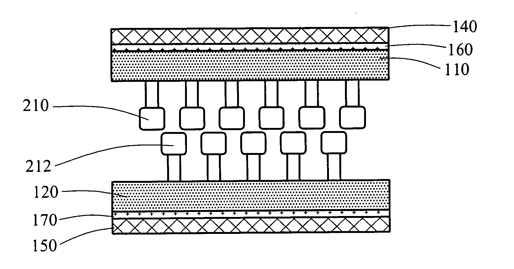
[0028] Referring to FIG. 2A, it shows a schematic view of an interconnect structure of the integrated circuit according to the present invention. It can be seen from the drawing that the shape of the first pillars 210 and the second pillars 212 is the same, and the structure of pillars is constituted of a relatively thin pillar and a relatively thick pillar. FIG. 2B is a schematic view of the interconnect structure of FIG. 2A after interconnection. The interconnect structure can provide a superior interconnection effect. Since each pillar is tiny, the structure is flexible, such that the structure can be easily disconnected just by tearing along the edge.

[0029]FIG. 3 is a schematic view of an interconnect structure according to a third embodiment of the present invention. The first pillars 312 and second pillars 310 are hook-shaped. And the same structures at two sides can be engaged closely after interconnection. Also, FIG. 4 is a schematic view of an interconnect structure accordi...


PUM


Abstract

An interconnect structure of an integrated circuit and manufacturing method therefor are provided, relating to an interconnect structure of flexible packaging. The interconnect structure includes a first and a second conductive pads. A plurality of tiny and conductive first pillars is respectively formed on the first and second pads. With different densities and thicknesses of the first and second pillars, a contact strength can be generated when the pillars interconnecting with each other, such that the pillars are connected closely. Furthermore, the interconnect structure can also be used to connect with fibers made of conductive materials. Moreover, the higher the density of the pillars, the stronger the contact strength. And, electronic substrates and active or passive electronic elements can be stuck on the other side of each pad. Therefore, the interconnect structure can maintain flexibility and have high reliability without being enhanced by any thermosetting polymer.

Description

CROSS-REFERENCE TO RELATED APPLICATIONS [0001] This non-provisional application claims priority under 35 U.S.C. § 119(a) on Patent Application No(s). 094142678 filed in Taiwan, R.O.C. on Dec. 2, 2005, the entire contents of which are hereby incorporated by reference. BACKGROUND OF THE INVENTION [0002] 1. Field of Invention [0003] The present invention relates to an interconnect structure and manufacturing method therefor, and more particularly relates to an interconnect structure of an integrated circuit and manufacturing method therefor. [0004] 2. Related Art [0005] Recently, with the rapid development of technology, people enjoy a better life due to the active research and hard work of scientists. It is the most urgent subject in the future for scientists to research, develop, and manufacture compact and light in weight devices which are safe, environment friendly, portable, and wearable along with the development of multifunctional electronic products. Therefore, it becomes one o...

Claims


Application Information

Patent Timeline
IPC IPC(8): H01L21/4763H01L23/48
CPCH01L23/49811H01L24/11H01L24/12H01L24/16H01L24/90H01L2224/1147H01L2224/13099H01L2924/14H05K3/326H05K2201/0373H05K2201/209H01L2224/81899H01L2224/16237H01L2224/81193H01L2224/81385H01L2924/01006H01L2924/014H01L2224/11902H01L2924/351H01L2224/16105H01L2224/81194H01L2224/1411H01L2224/16106H01L2224/023H01L2224/83899H01L2224/83897H01L2224/81897H01L24/81H01L24/83H01L2924/00H01L2924/0001H01L2924/00012
Inventor HSU, YUNG-YUCHEN, CHIH-YUANLIAU, SHYI-CHINGLEE, MIN-LINTAIN, RA-MINFENG, RONG-CHANG
Owner IND TECH RES INST
Why Eureka
Try Eureka