Light emitting element array and image forming apparatus

an array and light-emitting element technology, applied in the direction of electrical apparatus, semiconductor devices, printing, etc., can solve the problems of reducing the light emission efficiency in the low current injection region, the influence of the active layer exposure on the light emission efficiency, and the waste of current components. , to achieve the effect of improving the electrical isolation at the element isolation region, and reducing the leak current between elements

Inactive Publication Date: 2007-06-14
CANON KK
View PDF12 Cites 19 Cited by
  • Summary
  • Abstract
  • Description
  • Claims
  • Application Information

AI Technical Summary

Benefits of technology

[0008] However, when the opposite conductive type layer present under the active layer is etched, the active layer is inevitably partly exposed at an element side surface. In particular, when an AlGaAs layer is formed as the active layer, non-radiative recombination occurs at the exposed portion. Since this non-radiative recombination itself does not contribute to light emission, the current component through the non-radiative recombination is just wasted. That is, when the active layer is partly exposed, as a result, the light emission efficiency in a low current injection region is decreased.
[0012] The present invention aims to solve the above problems and, in particular, it provides a light emitting element having a low leak current and excellent light emission efficiency.
[0014] Moreover, according to the present invention, when the resistive layer is provided on the active layer, the electrical isolation at the element isolation region can be improved, and a leak current between elements can be decreased. That is, a wasted current component in a low current injection region can be decreased, and as a result, an element array having high light emission efficiency can be realized. Also, since the isolation of the light emitting elements is performed by etching, and the etching is stopped by the resistive layer, the active layer is not exposed, and hence the non-radiative component can be decreased. Accordingly, in addition to the above-described effect of suppressing a leak current, since the wasted current component which has no contribution to light emission can be decreased, an element array having high light emission efficiency can be realized. In addition, according to the present invention, since the etching stop layer is further provided, highly accurate and highly uniform element formation and element isolation can be realized without being affected by etching time.

Problems solved by technology

However, when the opposite conductive type layer present under the active layer is etched, the active layer is inevitably partly exposed at an element side surface.
Since this non-radiative recombination itself does not contribute to light emission, the current component through the non-radiative recombination is just wasted.
That is, when the active layer is partly exposed, as a result, the light emission efficiency in a low current injection region is decreased.
Accordingly, the influence on the light emission efficiency caused by the exposure of the active layer is serious as compared to that of a general light emitting diode.
As a result, degradation in element properties and in the element itself may occur due to heat generation in some cases.
However, for the Zn diffusion, a high-temperature and long-time process (for example, by a heat treatment at 700° C. for 30 minutes) must be performed.

Method used


Image

  • Light emitting element array and image forming apparatus
  • Light emitting element array and image forming apparatus
  • Light emitting element array and image forming apparatus

Examples


first embodiment

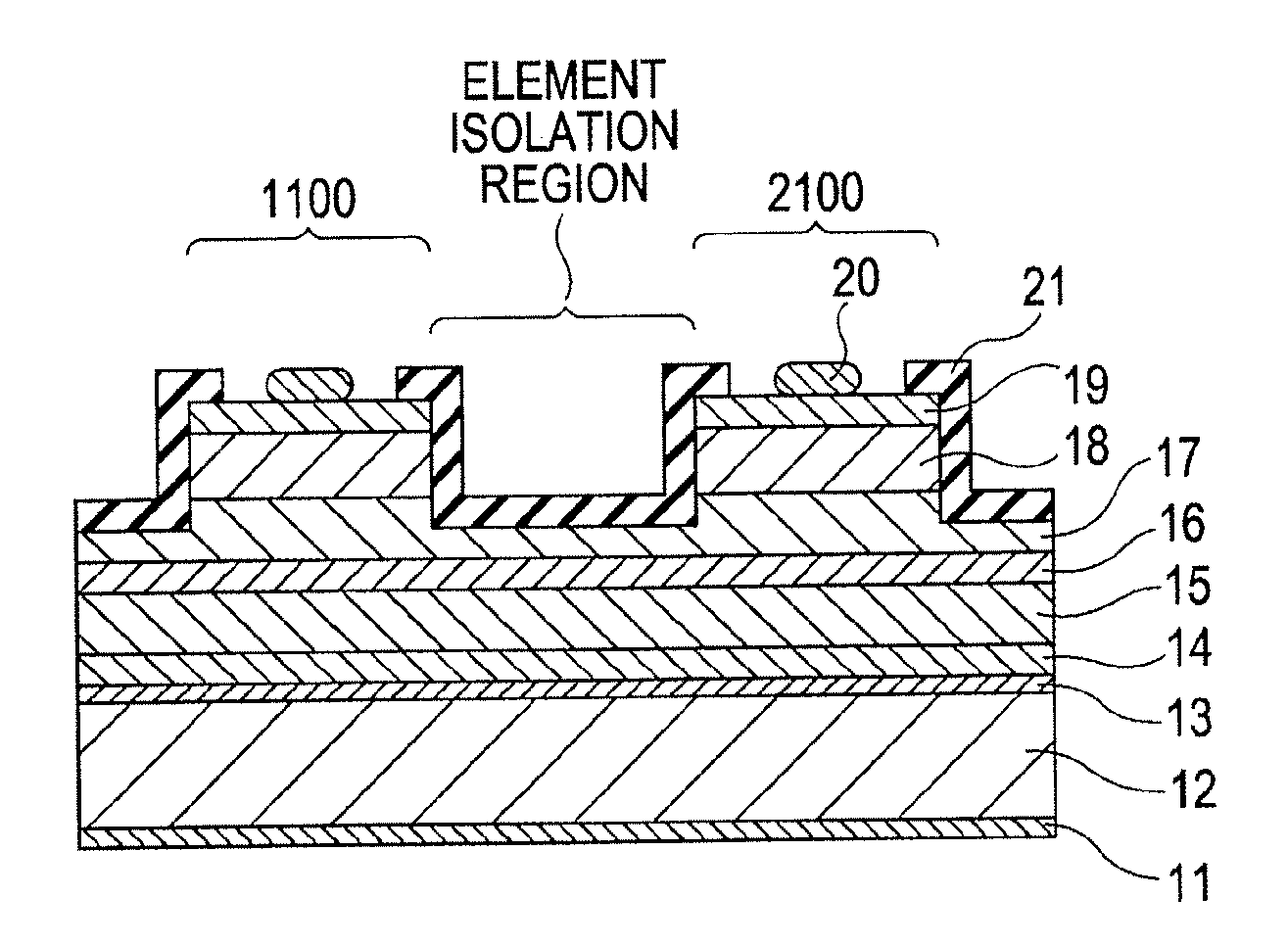
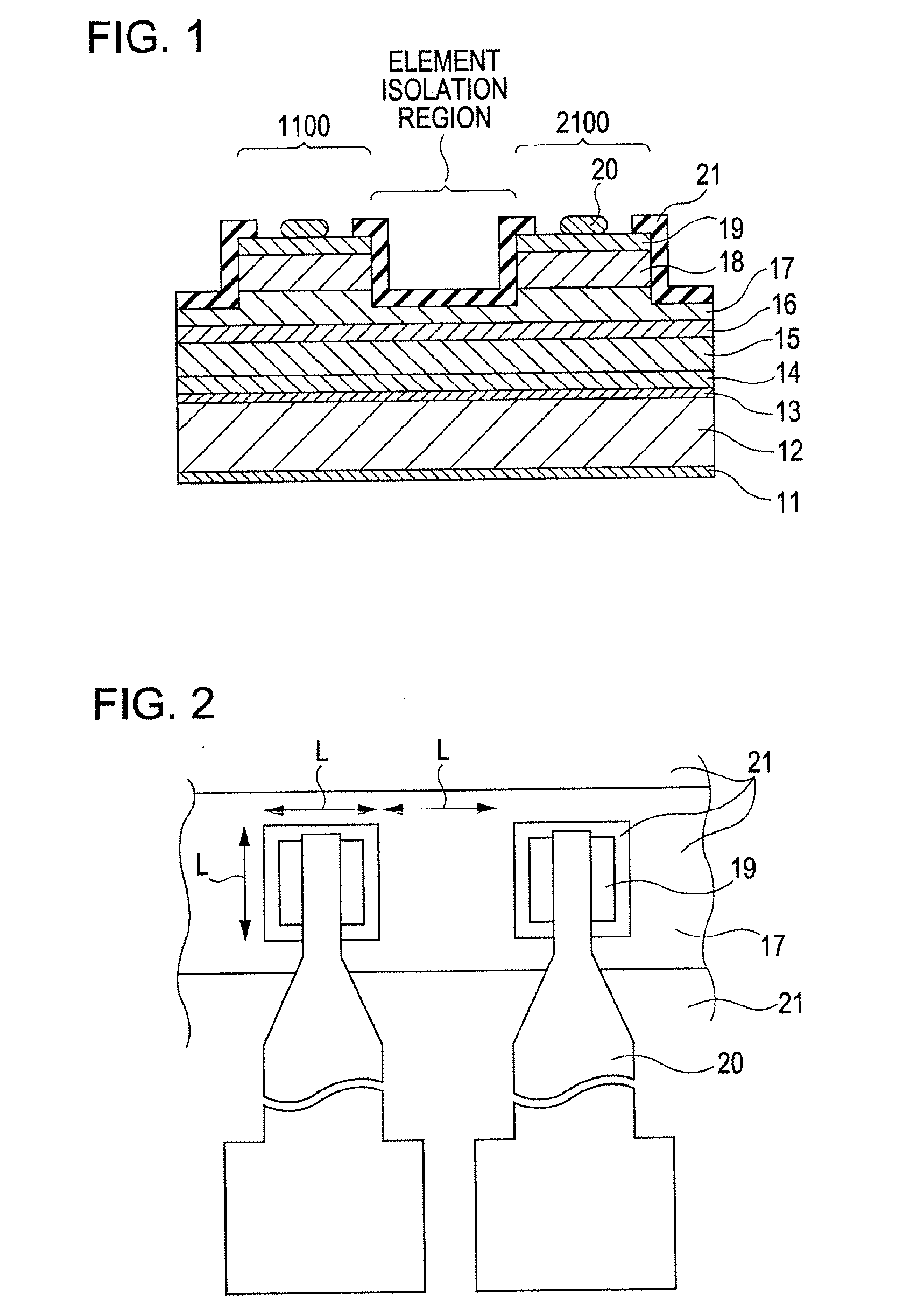
[0028]FIG. 1 is a cross-sectional view of a light emitting element array of a first embodiment according to the present invention. In this embodiment, the light emitting element array has an n-side electrode 11, an n-type Si substrate 12, a metal mirror 13, an n-type GaAs layer 14, an n-type AlGaAs layer 15, an AlGaAs quantum well active layer 16, and an undoped AlGaAs resistive layer 17. In addition, on the undoped AlGaAs resistive layer 17 are provided a p-type AlGaAs layer 18 functioning as a carrier injection layer (a hole injection layer in this embodiment), a p-type GaAs layer 19, a p-side electrode 20, and an insulating film 21. In order to achieve the element isolation, the p-type GaAs layer 19 and the p-type AlGaAs layer 18 are sequentially etched, and the AlGaAs resistive layer 17 is also partly etched. In FIG. 1, reference numeral 1100 indicates a first light emitting element region, and reference numeral 2100 indicates a second light emitting element region.

[0029]FIG. 2...

second embodiment

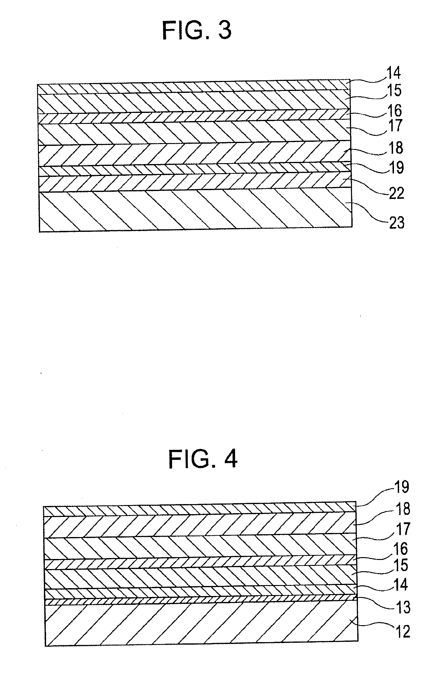
[0046]FIG. 7 is a cross-sectional view of a light emitting element array of the second embodiment according to the present invention. In FIG. 7, the same reference numerals as in FIG. 1 designate the same constituent elements, and a description thereof will be omitted. In this embodiment, which is different from that described with reference to FIG. 1, an AlInGaP etching stop layer 25 is formed on the AlGaAs resistive layer 17. Since etching is automatically stopped by this AlInGaP etching stop layer 25, more uniform element isolation can be realized.

[0047] In a process for forming the element array of this embodiment, as shown in FIG. 8, an element layer structure, which is inverse to a layer structure shown in FIG. 7, is formed on the GaAs substrate 23 by epitaxial growth. In this process, the AlAs selective etch separation layer 22 is inserted under the entire inverse structure. This AlAs selective etch separation layer 22 will be selective-etched in a subsequent step, so that t...


PUM


Abstract

A light emitting element array including an active layer commonly used for light emitting element regions, carrier injection layers which are electrically isolated from each other and which are provided in the respective light emitting element regions, and a resistive layer which has a resistance higher than that of the carrier injection layers and which is provided between the active layer and the carrier injection layers.

Description

BACKGROUND OF THE INVENTION [0001] 1. Field of the Invention [0002] The present invention relates to a light emitting element array and an image forming apparatus utilizing that array. [0003] 2. Description of the Related Art [0004] As an exposure light source embodying a light emitting element array in which several thousands of light emitting diodes and the like are arranged in a predetermined manner has been used for an electrophotographic printer. For example, element structures each formed of several AlGaAs layers are provided on a compound semiconductor substrate made of GaAs, and an array configuration is formed from the element structures (see Japanese Patent No. 3185049). [0005] When a light emitting element array is used for printers, it is necessary to determine an element size and a distance between elements in accordance with a desired degree of print resolution. When the resolution is represented by 600 dots per inch, the element size must be 40 μm square or less, and ...

Claims


Application Information

Patent Timeline
Patent Type & Authority Applications(United States)
IPC IPC(8): H01L33/00H01L31/12H01L33/06H01L33/08H01L33/10H01L33/30
CPCB41J2/45H01L27/153H01L33/145H01L2924/0002Y10S257/918H01L2924/00
Inventor TAKEUCHI, TETSUYA
Owner CANON KK
Why Eureka
Try Eureka