Systems and methods for inspecting a wafer with increased sensitivity

Active Publication Date: 2007-06-14
KLA TENCOR CORP
View PDF10 Cites 11 Cited by
  • Summary
  • Abstract
  • Description
  • Claims
  • Application Information

AI Technical Summary

Benefits of technology

[0021] Another embodiment relates to a gas flow subsystem configured to be coupled to an inspection system. The gas flow subsystem is configured to replace a gas located proximate to a spot on a wafer illuminated by the inspection system during inspection with a medium that scatters less of the light than the gas thereby increasing the sensitivity of the inspection system. The gas flow subsystem may be further configured as described herein.
[0022] An additional embodiment relates to a method f

Problems solved by technology

For instance, as the dimensions of semiconductor devices decrease, detection of defects of decreasing size has become necessary since even relatively small defects may cause unwanted aberrations in the semiconductor devices.
The best performance of most commercially available inspection systems does not meet these sensitivity and throughput perf

Method used


Image

  • Systems and methods for inspecting a wafer with increased sensitivity
  • Systems and methods for inspecting a wafer with increased sensitivity
  • Systems and methods for inspecting a wafer with increased sensitivity

Examples


example

Background Atmospheric Scattering with Normal Air and Helium Atmospheres

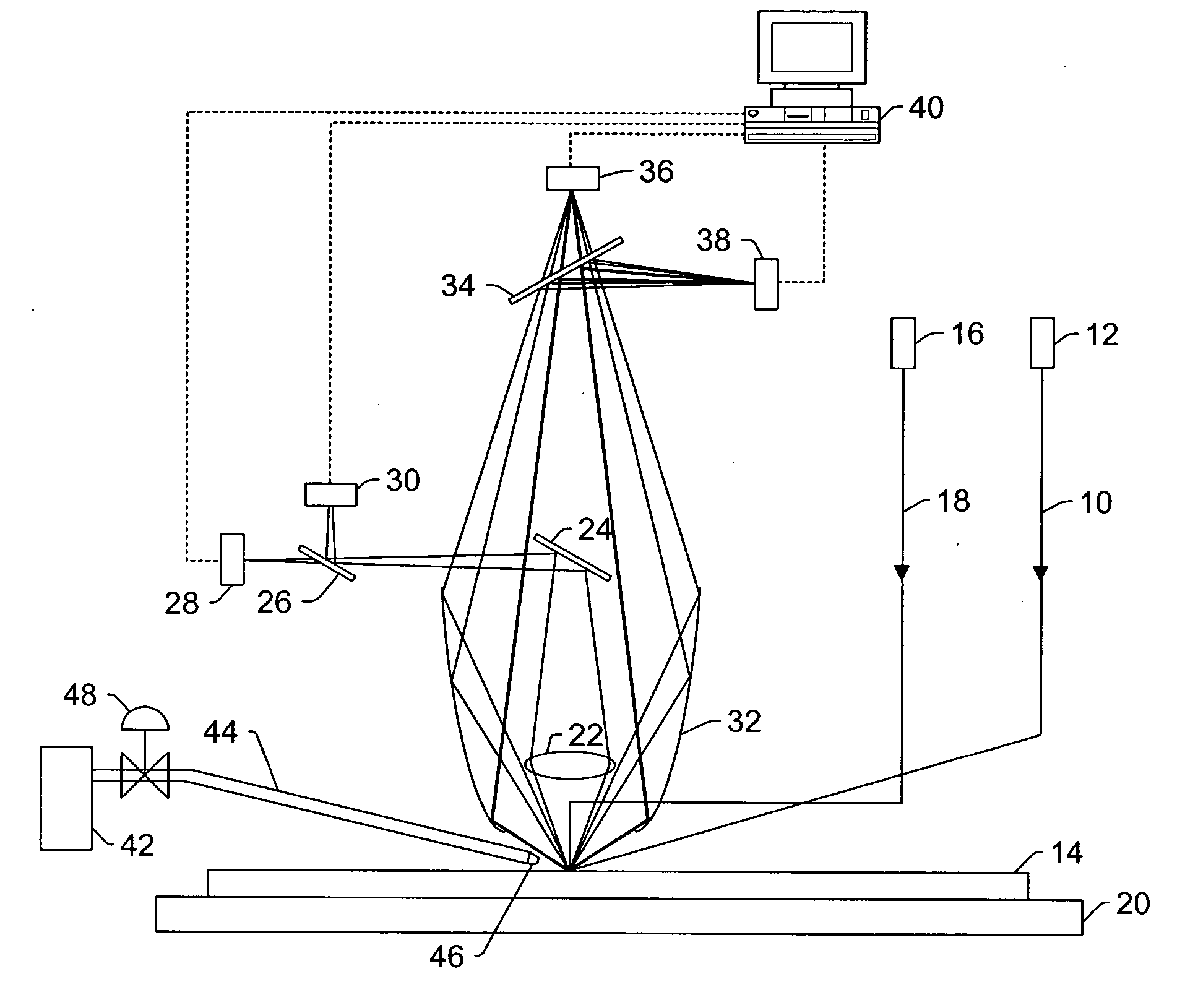
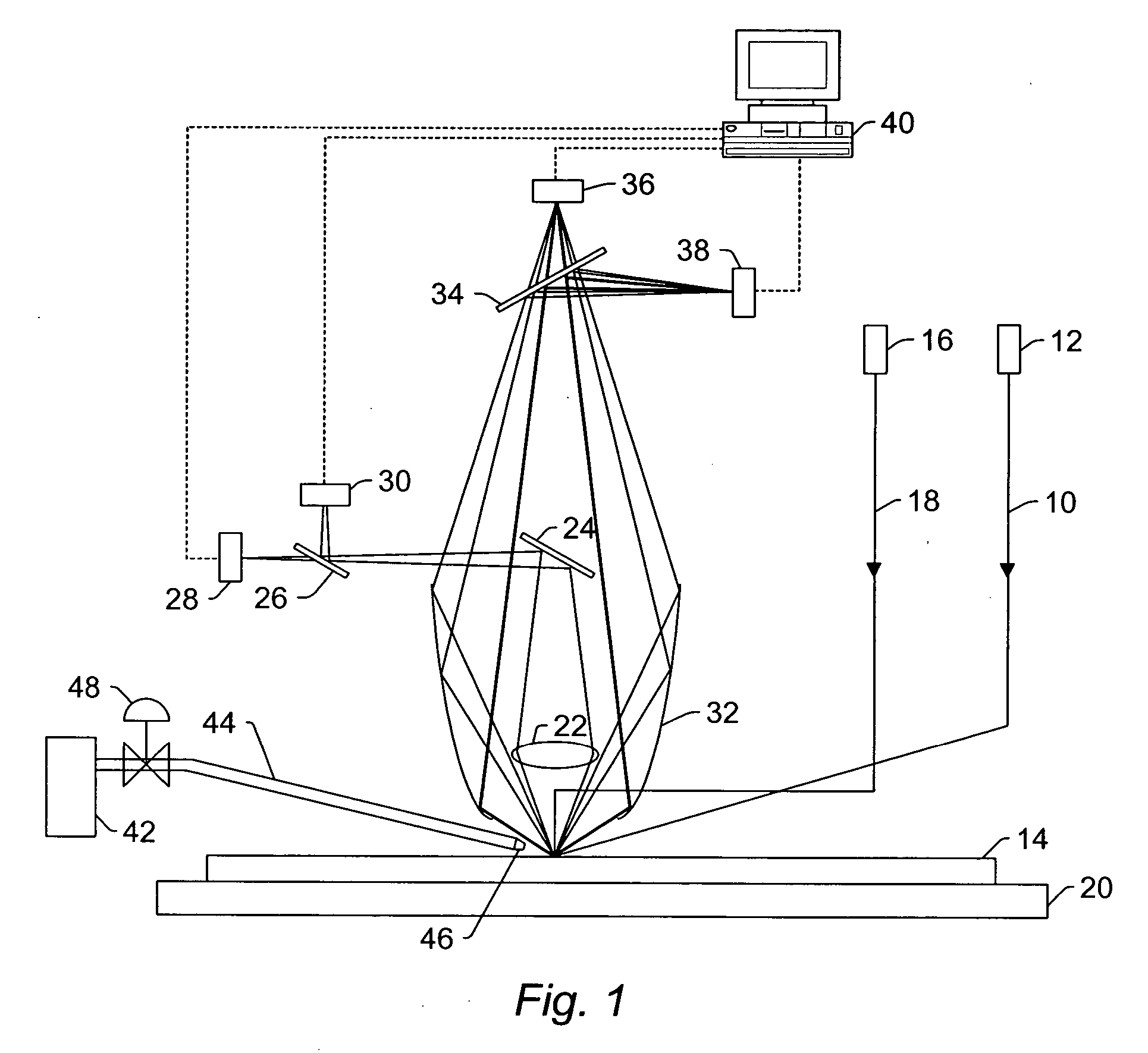
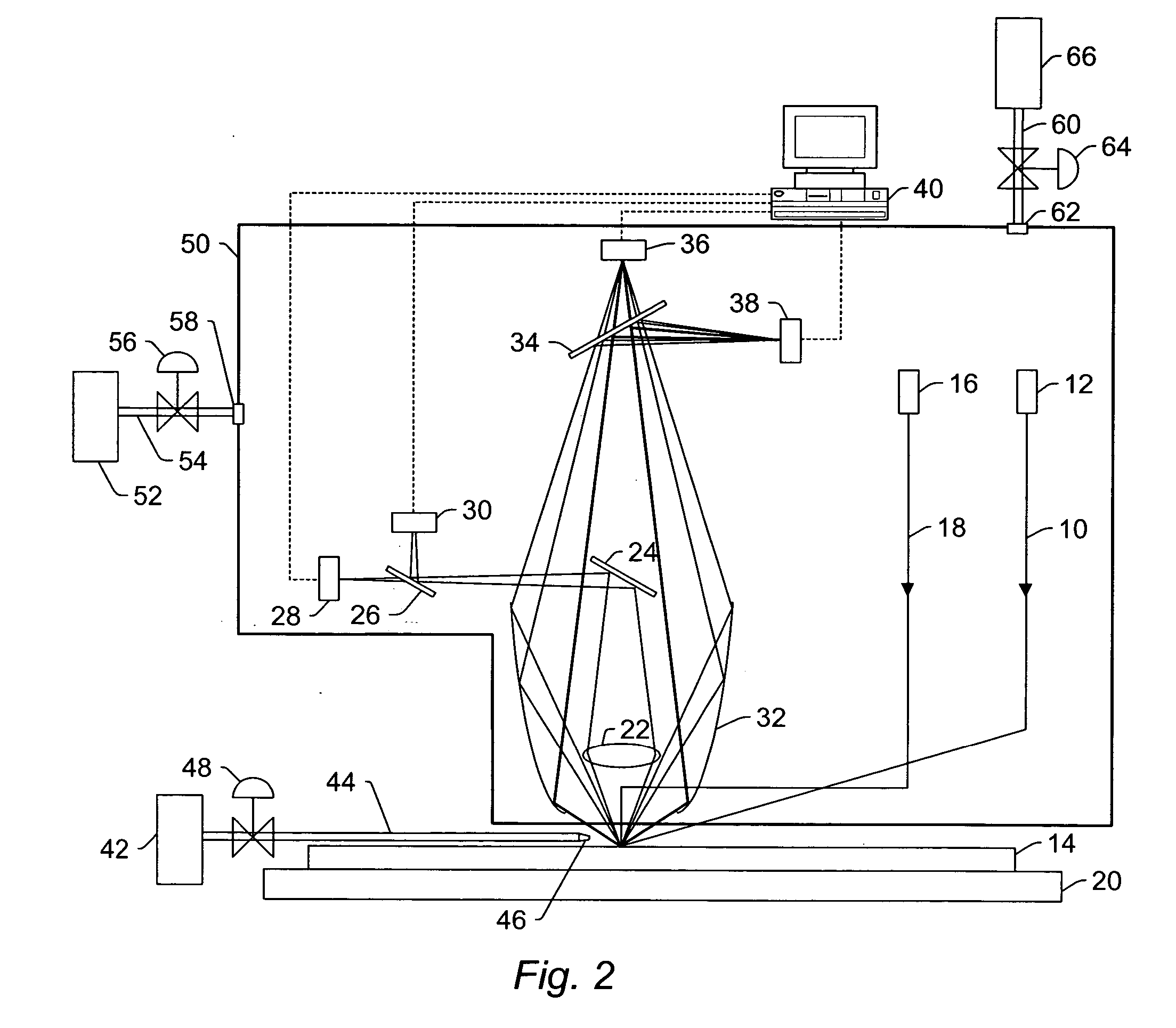
[0088] The background atmospheric scattering of normal air and helium atmospheres was measured using an SP2 tool that included a 350 mW laser operating at a wavelength of 355 nm. The normal air atmosphere in the SP2 tool was replaced with a helium atmosphere by “flooding” the collector of the SP2 tool with high purity helium (>98% purity). The helium was provided to the system using a helium tank and a 400 mm long tube about 50 mm in diameter attached to the bottom of the wide collector (i.e., ellipsoidal mirror 32 described above). The helium was inserted about half way into the tube with an estimated flow rate on the order of 1 L / s. The helium flowed up into the collector thereby replacing some or most of the air in the collector. Openings in the middle section of the collector allowed the helium flow to “push” any residual air out of the collector. The scattering in the two different atmospheres was measured...


PUM


Abstract

Systems and methods for inspecting a wafer with increased sensitivity are provided. One system includes an inspection subsystem configured to direct light to a spot on the wafer and to generate output signals responsive to light scattered from the spot on the wafer. The system also includes a gas flow subsystem configured to replace a gas located proximate to the spot on the wafer with a medium that scatters less of the light than the gas thereby increasing the sensitivity of the system. In addition, the system includes a processor configured to detect defects on the wafer using the output signals.

Description

BACKGROUND OF THE INVENTION [0001] 1. Field of the Invention [0002] The present invention generally relates to systems and methods for inspecting a wafer with increased sensitivity. Certain embodiments relate to systems and methods for inspecting a specimen that include replacing a gas proximate to an illuminated spot on the wafer with a medium that scatters less light than the gas thereby increasing the sensitivity of the inspection. [0003] 2. Description of the Related Art [0004] The following description and examples are not admitted to be prior art by virtue of their inclusion in this section. [0005] Fabricating semiconductor devices such as logic and memory devices typically includes processing a specimen such as a semiconductor wafer using a number of semiconductor fabrication processes to form various features and multiple levels of the semiconductor devices. For example, lithography is a semiconductor fabrication process that typically involves transferring a pattern to a re...

Claims


Application Information

Patent Timeline
IPC IPC(8): G01N21/88
CPCG01N21/9501G01N21/88H01L22/00
Inventor HALLER, KURT L.SHORTT, DAVIDWOLTERS, CHRISTIAN
Owner KLA TENCOR CORP
Why Eureka
Try Eureka