Electronic device having low background luminescence, a black layer, or any combination thereof

Inactive Publication Date: 2007-06-21
EI DU PONT DE NEMOURS & CO
View PDF24 Cites 13 Cited by
  • Summary
  • Abstract
  • Description
  • Claims
  • Application Information

AI Technical Summary

Benefits of technology

[0005] An electronic device or a process of forming an electronic device can include a first electrode configured to achieve low Lbackground or include a black layer. In a first aspect, an electronic device can include a substrate including a user surface. The electronic device can also include a first electrode that i

Problems solved by technology

Reflected ambient radiation can be a problem to users of the displays.
The high reflectivity can result in poor readability or low contrast of the devices in lighted environments, and particularly when used outdoors.
However, circular polarizers can block about 6

Method used


Image

  • Electronic device having low background luminescence, a black layer, or any combination thereof
  • Electronic device having low background luminescence, a black layer, or any combination thereof
  • Electronic device having low background luminescence, a black layer, or any combination thereof

Examples


example 1

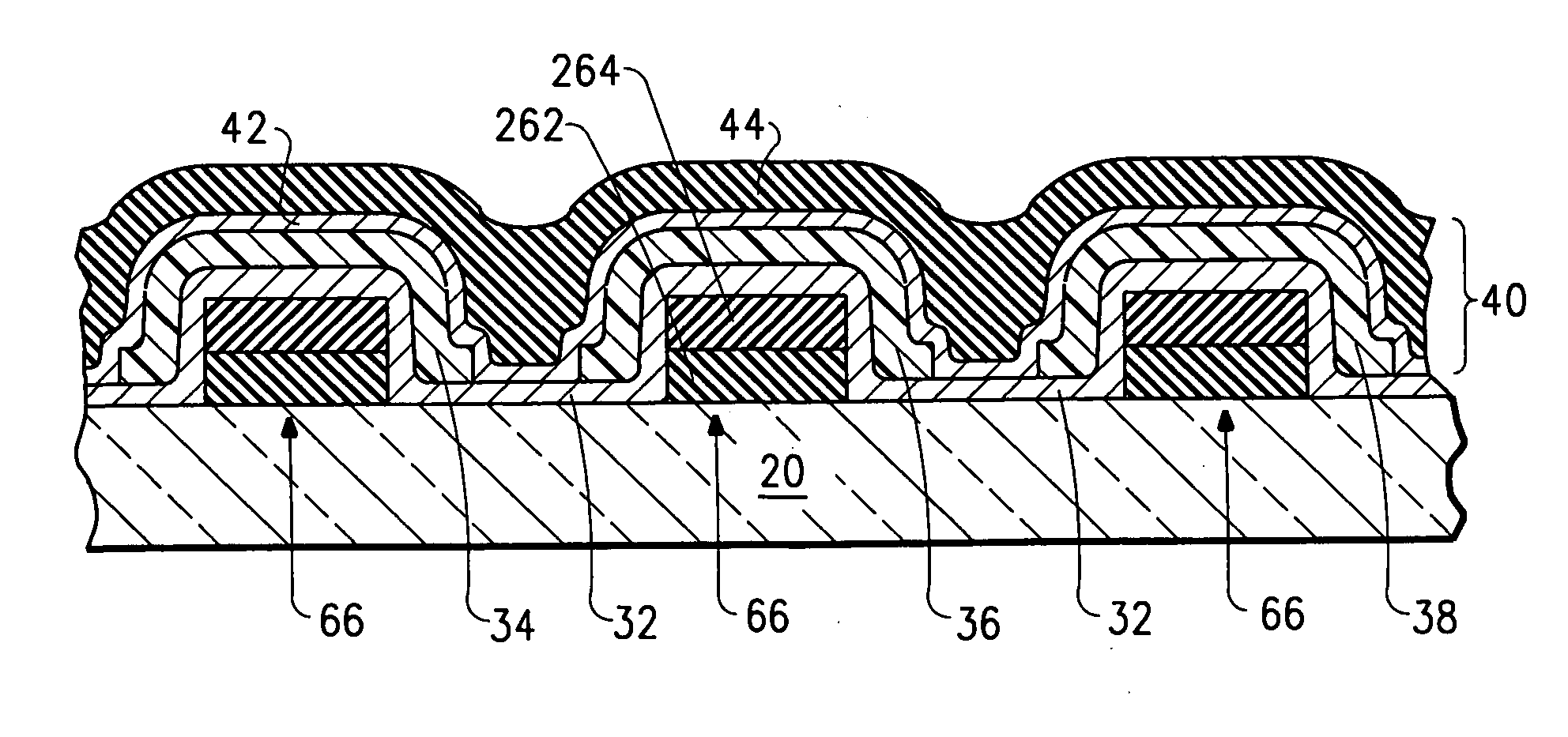
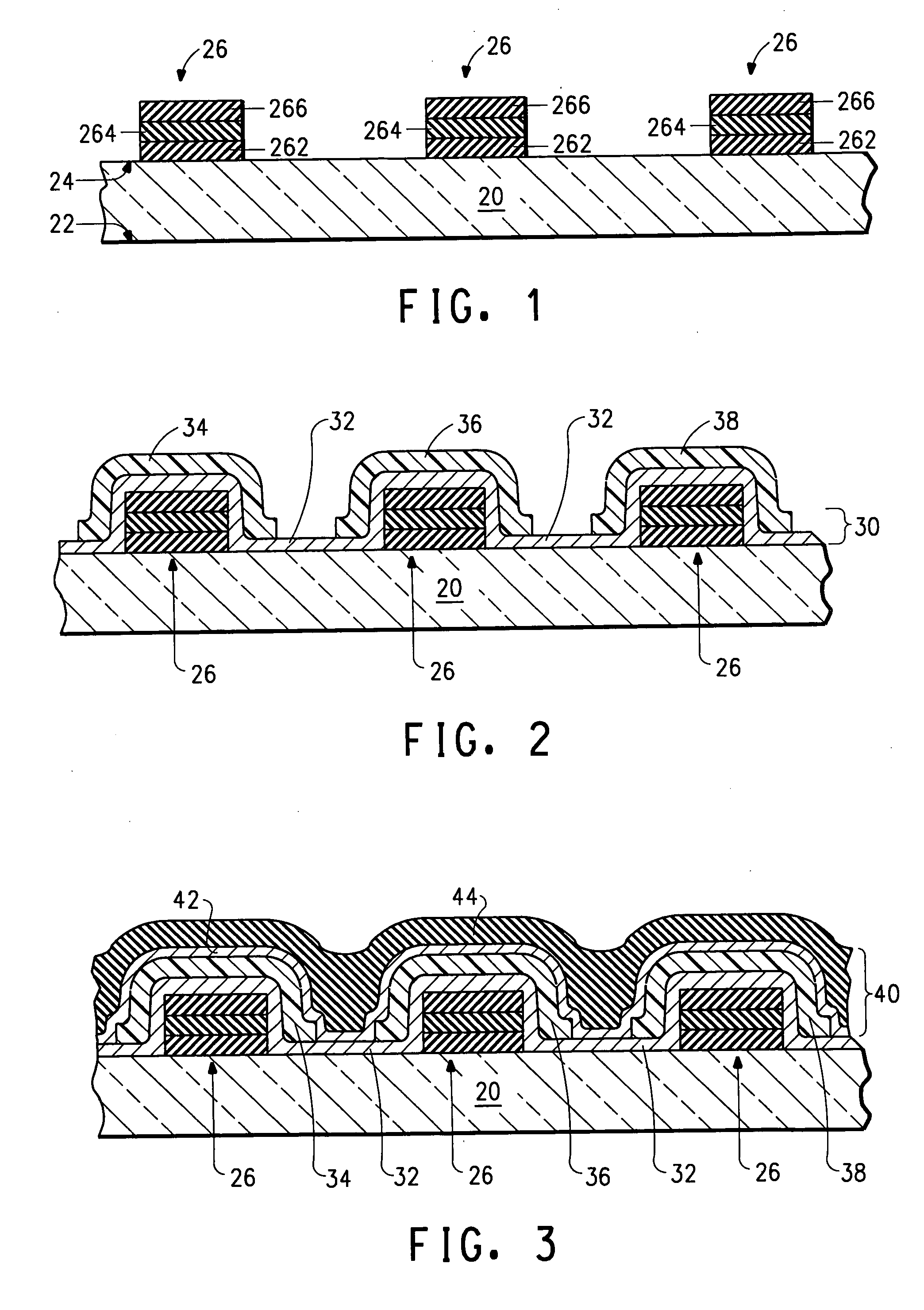
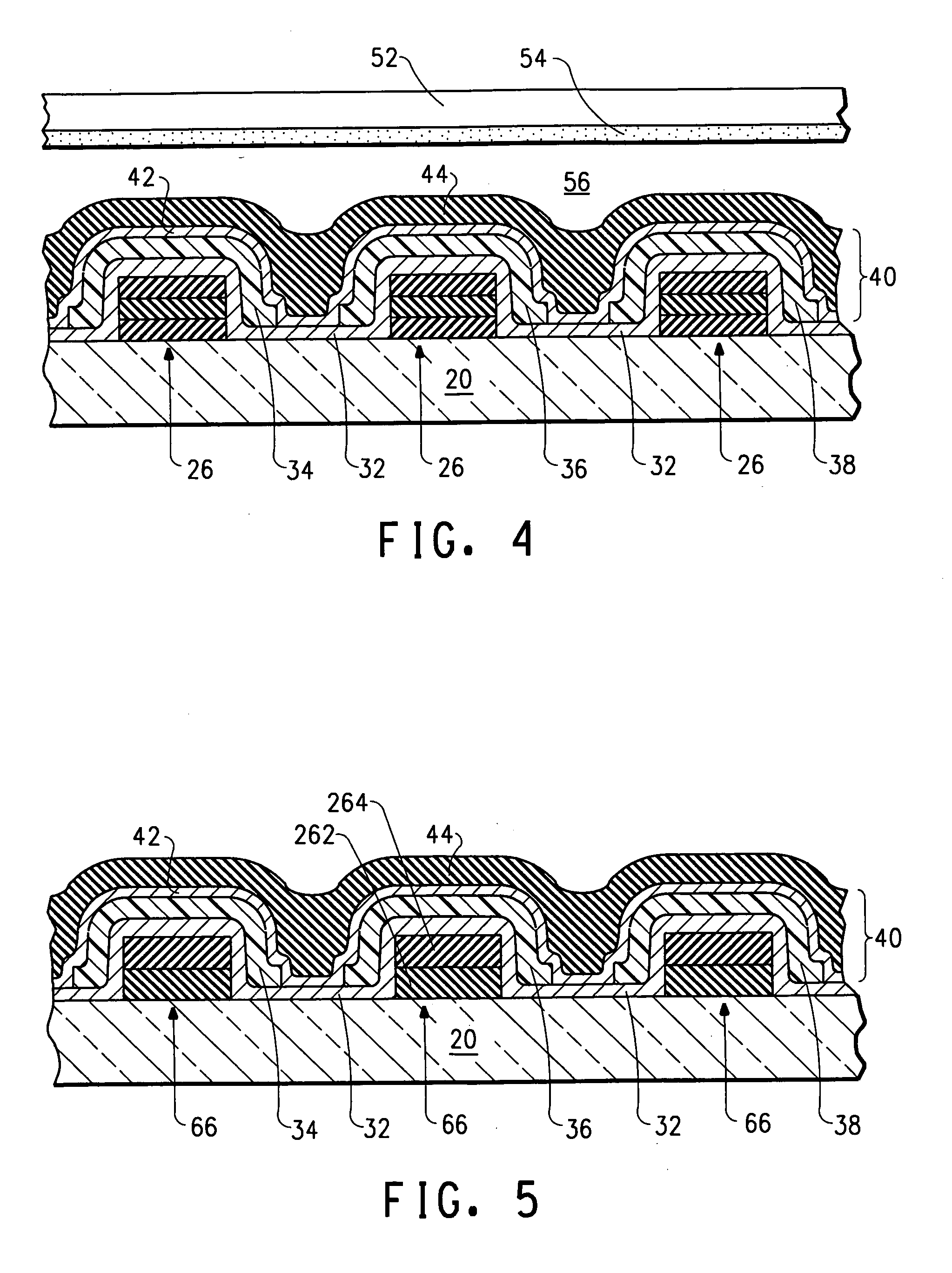
[0092] Example 1 demonstrates that the composition, thickness, or both of one or more layers within a cathode may not be well suited to achieve low Lbackground. An electronic device can be fabricated with a cathode that includes a Sm layer in the cathode. The cathode can include a sandwich of Ba / Al / Sm / Al or LiF / Al / Sm / Al, depending on whether Ba or LiF is used as the low work function layer. FIGS. 6 through 8 include graphs for luminance, ClEy (color), and reflectance for the cathode including the Sm layer. The luminance and color properties at varying thicknesses of the Sm layer are acceptable, but the minimum reflectance is relatively high and at a frequency (approximately 470 nm) within the blue light spectrum. The minimum reflectance is higher than 20%. The human eye has less sensitivity to radiation within the blue light spectrum (400 to 500 nm) as compared to the green light spectrum (500 to 600 nm).

example 2

[0093] Example 2 demonstrates that the composition, thickness or both of one or more layers within an anode may be more effective to achieve low Lbackground as compared to the cathode in Example 1. An electronic device can be fabricated with a cathode that includes a Ru or Cr layer in the anode. The anode can include a sandwich of ITO / Ru / ITO or ITO / Cr / ITO. FIGS. 9 through 11 include graphs for luminance, ClEy, and reflectance for the anode including the Ru or Cr layer. Luminance is not as good for the cathode in Example 1. However, the color improves and the minimum reflectance is significantly lower, and is very low in the eye sensitivity range, which corresponds to the green light spectrum (wavelength range 500 to 600 nm). The minimum reflectance is less than 10%, and in a particular embodiment is less than 5%. Thus, the anode of Example 2 achieves a lower Lbackground than the cathode of Example 1.

[0094] Note that not all of the activities described above in the general descripti...


PUM


Abstract

An electronic device or a process of forming an electronic device can include a first electrode configured to achieve low Lbackground or include a black layer. An electronic device can include a substrate including a user surface. The electronic device can also include a first electrode that includes a first layer, a second layer, and a third layer. The second layer can lie between the first and third layers, and the first electrode can be configured to achieve low Lbackground. The electronic device can further include a second electrode lying farther from the user surface as compared to the first electrode. In another embodiment, a first electrode can include a first layer and a second layer. The second layer can set the work function of the electrode, and the second layer can be a black layer. Processes can be used to form the electronic devices.

Description

FIELD OF THE DISCLOSURE [0001] This disclosure relates in general to electronic devices, and more particularly, to an electronic device having low background luminescence, a black layer, or any combination thereof. DESCRIPTION OF THE RELATED ART [0002] An electronic device can include a liquid crystal display (“LCD”), an organic light-emitting diode (“OLED”) display, or the like. LCDs and OLED displays are promising technologies for flat panel display applications. Reflected ambient radiation can be a problem to users of the displays. One or more materials used for electrodes within the displays can have mirror-like reflectivity if its thickness is over 20 nanometers. The high reflectivity can result in poor readability or low contrast of the devices in lighted environments, and particularly when used outdoors. [0003] An attempt to solve the reflection problem is to place a circular polarizer in front of an OLED display panel. However, circular polarizers can block about 60% of the ...

Claims


Application Information

Patent Timeline
IPC IPC(8): H01L23/48H01J1/62
CPCH01L51/442H01L51/5206H01L51/5281Y02E10/549H01L2924/0002H01L2924/00H10K30/82H10K50/816H10K50/865H10K50/86H01L31/022466H10K50/81
Inventor PRAKASH, SHIVA
Owner EI DU PONT DE NEMOURS & CO
Why Eureka
Try Eureka