Modulation of stress in stress film through ion implantation and its application in stress memorization technique

a stress film and stress technology, applied in the manufacturing of semiconductor/solid-state devices, basic electric elements, electrical equipment, etc., can solve the problems of signal propagation time and susceptibility, the length of propagation paths, and the cost of devices containing chips, so as to increase the stress in the channel region

Inactive Publication Date: 2007-06-21
CHARTERED SEMICONDUCTOR MANUFACTURING
View PDF13 Cites 42 Cited by
  • Summary
  • Abstract
  • Description
  • Claims
  • Application Information

AI Technical Summary

Benefits of technology

[0019] performing an anneal of the substrate and stress layer whereby the impla

Problems solved by technology

That is, increased integration density and proximity of elements reduces the signal propagation path length and reduces signal propagation time and susceptibility to noise and increase of possible clock rates while the reduction in element size necessary for increased integration density increases to ratio of functionality which can be provided on a chip to

Method used


Image

  • Modulation of stress in stress film through ion implantation and its application in stress memorization technique
  • Modulation of stress in stress film through ion implantation and its application in stress memorization technique
  • Modulation of stress in stress film through ion implantation and its application in stress memorization technique

Examples


Embodiment Construction

I. Introduction

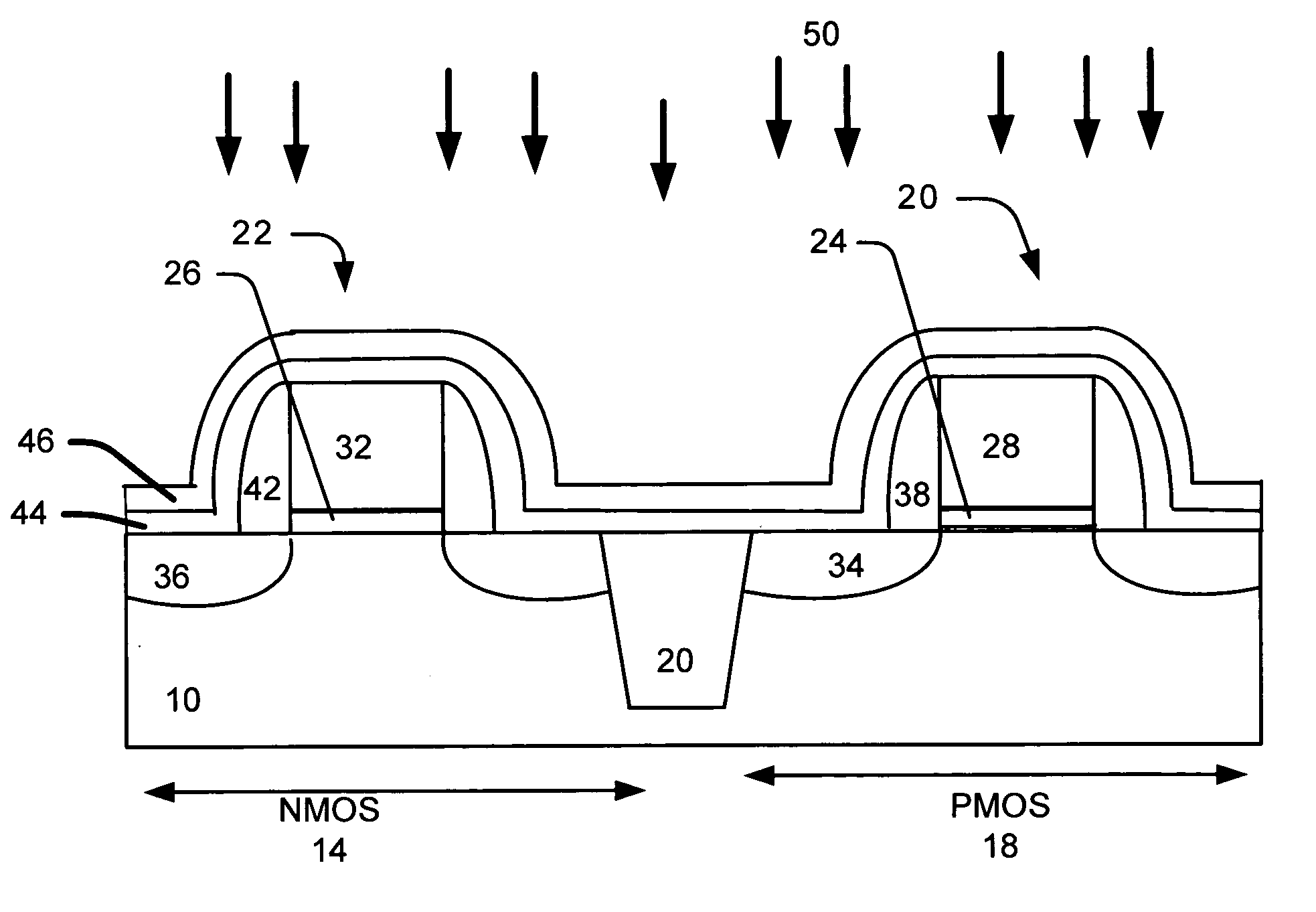
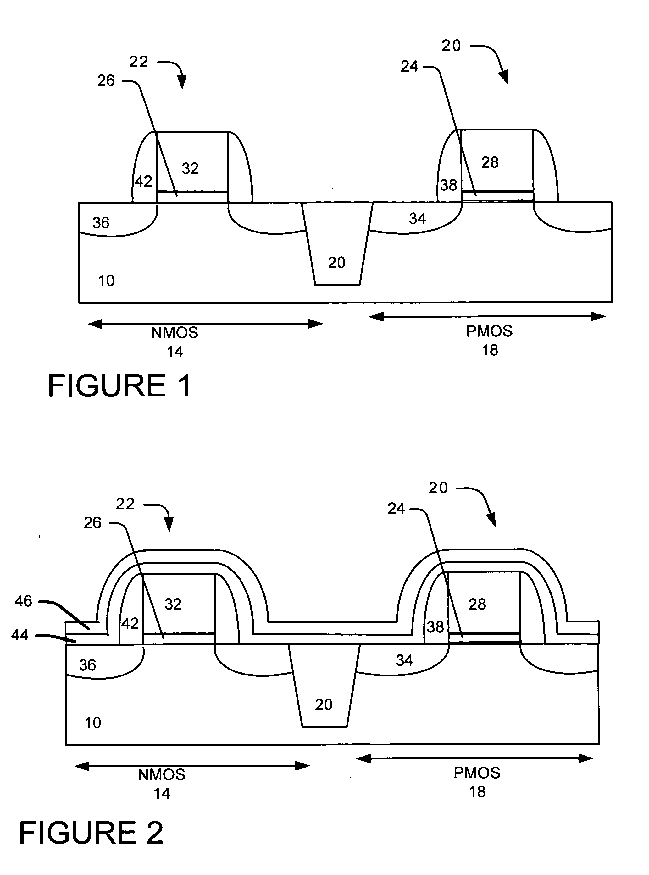
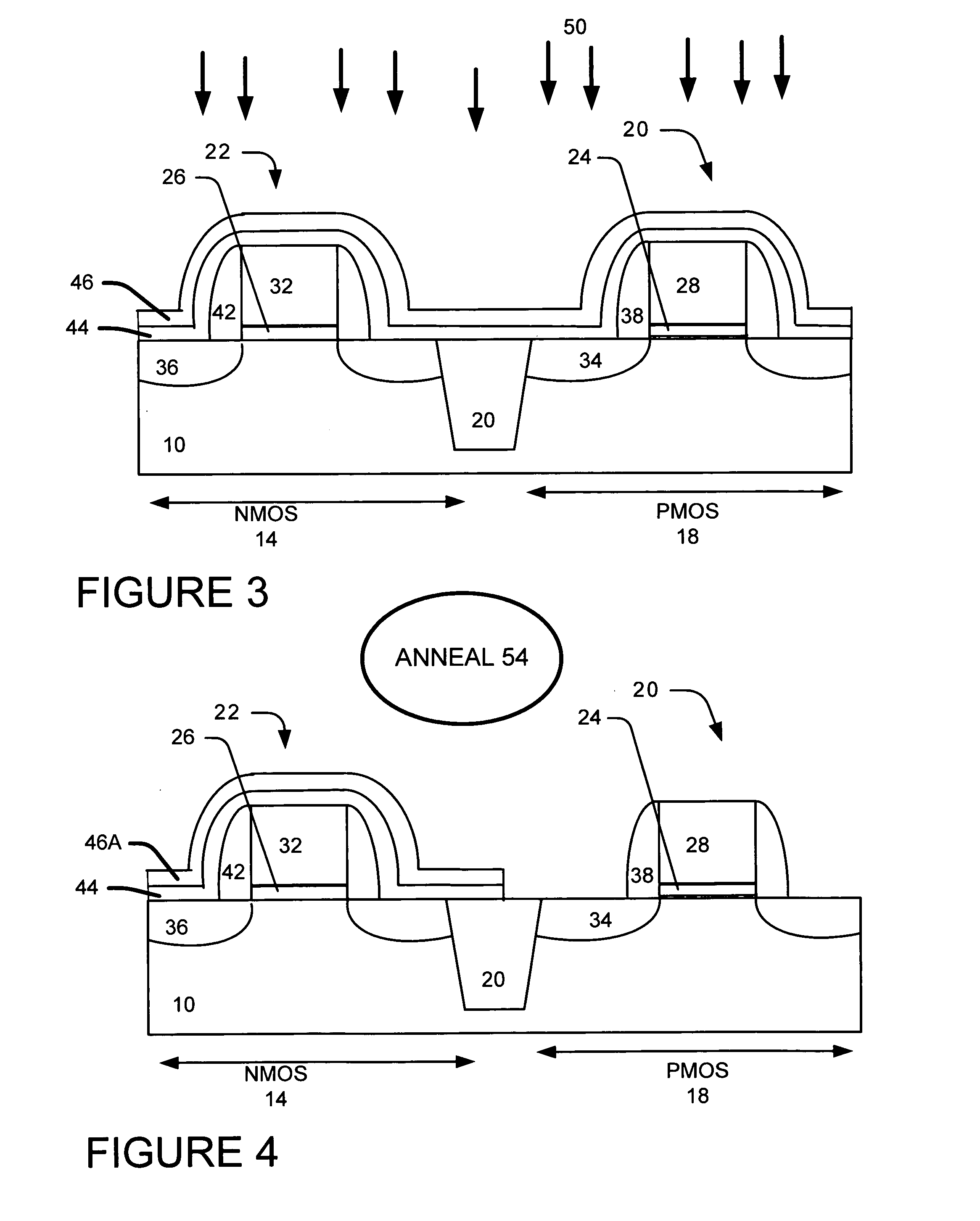
[0032] Some example embodiments of the invention provide a method to improve the performance of MOS devices by increasing the stress in the channel region. An example embodiment for a NMOS Transistor is to form a tensile stress layer (e.g., SiN) over a NMOS transistor. [0033] A gate dielectric layer and poly gate are formed. [0034] An ion implant is performed to amorphorize the gate so that the gate is comprised of amorphous Si. [0035] A important Ion implantation (I / I) is performed on the (SiN) stress layer that will initially relax the stress film but when combined with a subsequent anneal, will increase the tensile stress in the stress film higher than the initial starting stress. [0036] Then an anneal is performed that can serve two purposes: (i) increasing the tensile stress of the implanted stress film, (ii) crystallizes the silicon containing gate thus increasing the amount of stress from the stress layer that the gate retains / memorizes.

[0037] The Si containin...


PUM


Abstract

Some example embodiments of the invention provide a method to improve the performance of MOS devices by increasing the stress in the channel region. An example embodiment for a NMOS transistor is to form a tensile stress layer over a NMOS transistor. A heavy ion implantation is performed into the stress layer and then an anneal is performed. This increases the amount of stress from the stress layer that the gate retains/memorizes thereby increasing device performance.

Description

BACKGROUND OF INVENTION [0001] 1) Field of the Invention [0002] This invention relates generally to fabrication of semiconductor devices and more particularly to a method to change the stress in a stress layer over a FET device. [0003] 2) Description of the Prior Art [0004] Performance and economic factors of integrated circuit design and manufacture have caused the scale of elements (e.g. transistors, capacitors and the like) of integrated circuits to be drastically reduced in size and increased in proximity on a chip. That is, increased integration density and proximity of elements reduces the signal propagation path length and reduces signal propagation time and susceptibility to noise and increase of possible clock rates while the reduction in element size necessary for increased integration density increases to ratio of functionality which can be provided on a chip to the costs of production (e.g. wafer / chip area and process materials) per chip and, potentially, the cost of dev...

Claims


Application Information

Patent Timeline
IPC IPC(8): H01L21/8238
CPCH01L21/823807H01L21/823864
Inventor TEO, LEE WEEQUEK, ELGIN
Owner CHARTERED SEMICONDUCTOR MANUFACTURING
Why Eureka
Try Eureka