Method and apparatus for a printed circuit board using laser assisted metallization and patterning of a substrate

a printed circuit board and laser assisted technology, applied in the field of microelectronic structures made using, can solve the problems of low throughput, ineffective alignment budget, and compounding of possible alignment errors

Inactive Publication Date: 2007-06-28
INTEL CORP
View PDF6 Cites 30 Cited by
  • Summary
  • Abstract
  • Description
  • Claims
  • Application Information

AI Technical Summary

Problems solved by technology

However, techniques of the prior art such as those described above, may exhibit low throughput due to increased processing time, and, in addition, may be ineffective for meeting current

Method used


Image

  • Method and apparatus for a printed circuit board using laser assisted metallization and patterning of a substrate
  • Method and apparatus for a printed circuit board using laser assisted metallization and patterning of a substrate
  • Method and apparatus for a printed circuit board using laser assisted metallization and patterning of a substrate

Examples


Embodiment Construction

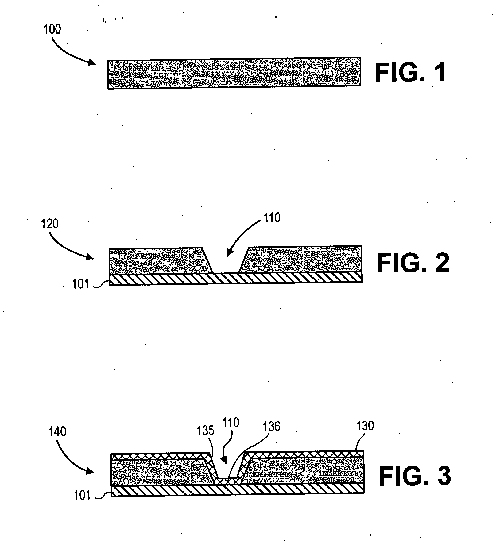
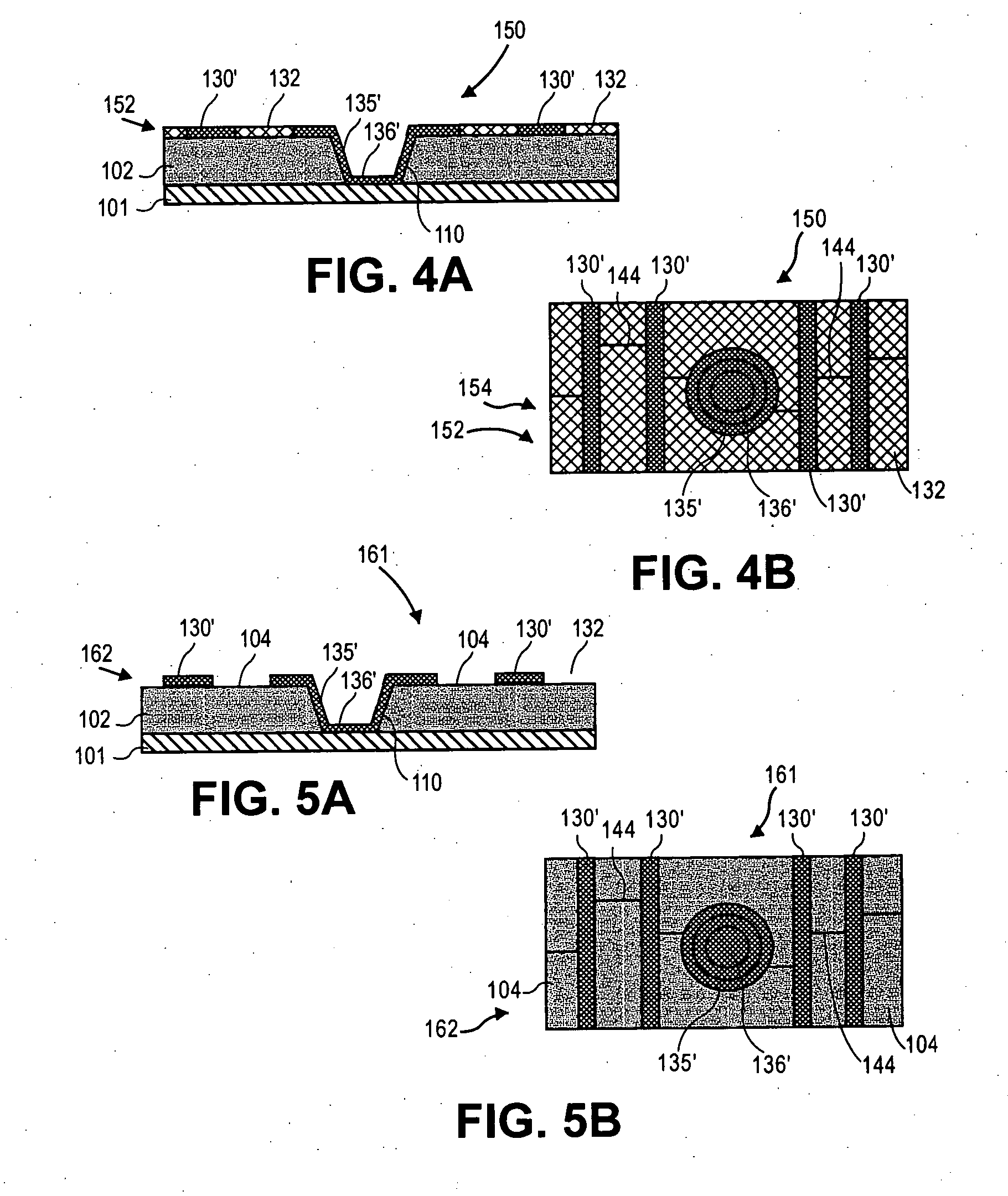
[0051] The embodiments discussed herein generally relate to a method, a printed circuit board and a system using laser assisted metallization and patterning. Referring to the figures, exemplary embodiments will now be described. The exemplary embodiments are provided to illustrate the embodiments and should not be construed as limiting the scope of the embodiments.

[0052] Various operations will be described as multiple discrete operations, in turn, in a manner that is most helpful in understanding the present invention, however, the order of description should not be construed as to imply that these operations are necessarily order dependent. In particular, these operations need not be performed in the order of presentation.

[0053] Referring now to FIG. 1 by way of example, embodiments of the present invention comprise providing a microelectronic substrate or panel, such as substrate 100, provided on a conductive layer 101 (see FIG. 2). The substrate may include a non-conductive ma...


PUM

PropertyMeasurementUnit
Electrical conductoraaaaaaaaaa

Abstract

A printed circuit is made by laser projection patterning a metal panel of a substrate, laminating a dielectric layer on the metal panel, laser irradiating the substrate to form vias in the substrate, laser activating a seed coat on the substrate, washing the seed coat from an unpatterned portion of the substrate, forming a patterned build-up layer on the substrate, and etching away a metal plating forming metal protrusions.

Description

Background [0001] 1. Field [0002] The embodiments relate to microelectronic structures, and more particularly to microelectronic structures made using laser assisted activation and patterning. [0003] 2. Description of the Related Art [0004] The state of the art provides numerous techniques for manufacturing a printed circuit board. The starting material is a microelectronic substrate, typically a dielectric board such as, for example, an ABF (Ajinomoto Build-up Film) layer, which may then be processed according to one of the numerous techniques mentioned above to provide the printed circuit. [0005] One such technique involves providing the dielectric layer, and then laser drilling via openings into the dielectric layer. Thereafter, the dielectric layer is roughened, subjected to chemical copper plating, such as electroless plating, to provide a thin layer of copper over the entire dielectric layer including on the walls of the via openings. A dry-film resist (DFR) is then laminated ...

Claims


Application Information

Patent Timeline
IPC IPC(8): H05K1/16
CPCH05K2201/0367Y10T29/49155H05K2201/09563H05K2201/09745H05K2203/0369H05K2203/0733H05K2203/107H05K2203/1476H01L21/486H01L23/49822H01L23/49827H05K3/027H05K3/185H05K3/4007H05K3/421H05K3/423H05K3/4661H01L2924/0002H05K2201/0394Y10T29/49156H01L2924/00H05K3/10H05K3/06
Inventor SALAMA, ISLAM A.
Owner INTEL CORP
Why Eureka
Try Eureka