Three-dimensional integrated circuit structure

a three-dimensional integrated circuit and integrated circuit technology, applied in the direction of basic electric elements, electrical equipment, semiconductor devices, etc., can solve the problems of reducing the size of the minimum required to make these components, the physical limits of the density that can be achieved in two dimensions, and the requirement of more complex designs, so as to improve the performance of the integrated circuit, simplify the manufacturing process, and reduce the delay of the circuit rc

Inactive Publication Date: 2007-06-28
TAIWAN SEMICON MFG CO LTD
View PDF11 Cites 70 Cited by
  • Summary
  • Abstract
  • Description
  • Claims
  • Application Information

AI Technical Summary

Benefits of technology

[0014] In the preferred embodiments of the present invention, PMOS and NMOS devices are fabricated on separate substrates, so that the fabrication processes are simplified. Since the materials and ...

Problems solved by technology

Although dramatic improvement in lithography has resulted in considerable improvement in 2D integrated circuit formation, there are physical limits to the density that can be achieved in two dimensions.
One of these limits is the minimum size needed to make these components.
Also, when more devices are put into one chip, more complex designs are required.
An addition...

Method used


Image

  • Three-dimensional integrated circuit structure
  • Three-dimensional integrated circuit structure
  • Three-dimensional integrated circuit structure

Examples


Embodiment Construction

[0021] The making and using of the presently preferred embodiments are discussed in detail below. It should be appreciated, however, that the present invention provides many applicable inventive concepts that can be embodied in a wide variety of specific contexts. The specific embodiments discussed are merely illustrative of specific ways to make and use the invention, and do not limit the scope of the invention.

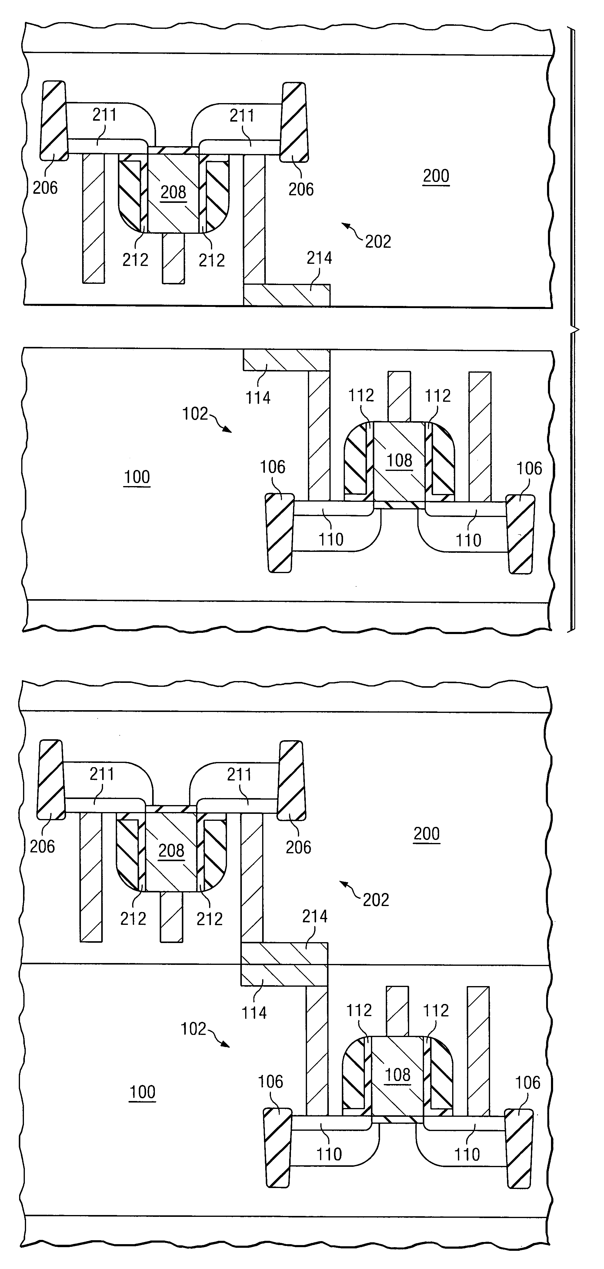
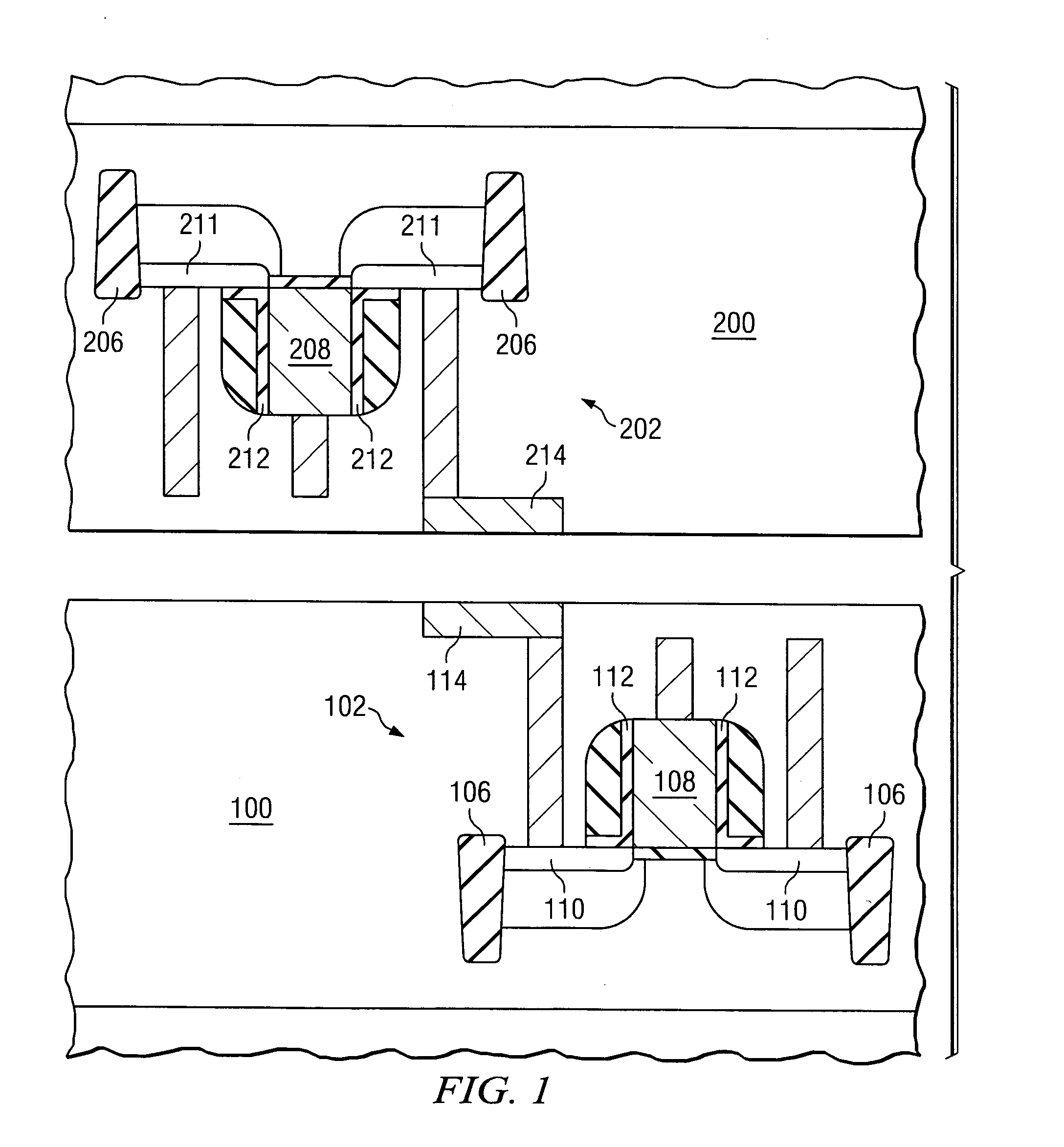
[0022]FIGS. 1 and 2 illustrate schematic cross-sectional views of a preferred embodiment of the present invention, wherein contact pads are pre-formed prior to bonding. In FIG. 1, a first substrate 100 and a second substrate 200 are provided. While in an ideal situation no PMOS devices are formed on substrate 100, in some embodiments, a limited number of PMOS devices might be formed on the substrate 100 to satisfy particular circuit requirements. Preferably, the first and second substrates are formed of different materials that are beneficial for NMOS and PMOS devices, resp...


PUM


Abstract

The preferred embodiments of the present invention provide a three-dimensional (3D) semiconductor structure and a method of forming the same. The 3D semiconductor structure includes a first substrate bonded to a second substrate. The first substrate includes substantially all NMOS devices. The second substrate includes substantially all PMOS devices. The substrates can be bonded face-to-face, face-to-back, or back-to-back. The method includes providing a first substrate and a second substrate, forming a first circuit comprising at least one NMOS device on the first substrate, wherein the first substrate includes substantially no PMOS devices, forming a second circuit comprising at least one PMOS device on the second substrate, wherein the second substrate includes substantially no NMOS devices, and bonding the first and second substrates after forming the first and second circuits.

Description

TECHNICAL FIELD [0001] This invention relates generally to integrated circuits, and more particularly to three-dimensional integrated circuits and manufacturing processes for forming the same. BACKGROUND [0002] Since the invention of the integrated circuit, the semiconductor industry has experienced continued rapid growth due to continuous improvements in the integration density of various electronic components (i.e., transistors, diodes, resistors, capacitors, etc.). For the most part, this improvement in integration density has come from repeated reductions in minimum feature size, which allows more components to be integrated into a given area. Additional improvement has come from increases in wafer size. [0003] These integration improvements are essentially two-dimensional (2D) in nature, in that the volume occupied by the integrated components is essentially on the surface of the semiconductor wafer. Although dramatic improvement in lithography has resulted in considerable impr...

Claims


Application Information

Patent Timeline
IPC IPC(8): H01L29/04
CPCH01L21/6835H01L21/8221H01L24/81H01L24/83H01L25/0657H01L25/50H01L27/0688H01L29/7833H01L2221/6834H01L2221/68363H01L2224/13147H01L2224/16145H01L2224/81203H01L2224/81801H01L2224/83191H01L2224/8385H01L2225/06513H01L2225/06541H01L2924/01005H01L2924/01015H01L2924/01029H01L2924/01073H01L2924/07802H01L2924/14H01L2924/19041H01L2924/19043H01L24/29H01L2224/9202H01L2924/01006H01L2924/01033H01L2924/0132H01L2924/01014H01L2924/01032
Inventor CHEN, HAI-CHINGHSIUNG, HAROLDLO, HENRY
Owner TAIWAN SEMICON MFG CO LTD
Why Eureka
Try Eureka