Semiconductor package having improved thermal performance

a technology of semiconductors and thermal performance, applied in the direction of semiconductor devices, semiconductor/solid-state device details, electrical apparatus, etc., can solve the problems of adversely affecting the operation of first and second mosfets, heat generated within the package, etc., and achieve the effect of improving the thermal performance of the package and increasing the amount of encapsulan

Active Publication Date: 2007-06-28
ALPHA & OMEGA SEMICON LTD
View PDF2 Cites 22 Cited by
  • Summary
  • Abstract
  • Description
  • Claims
  • Application Information

AI Technical Summary

Benefits of technology

[0008] The TSSOP-8 semiconductor package in accordance with the invention includes a common drain MOSFET pair bonded to a first lead frame die pad and an IC bonded to a second lead frame die pad. The first and second lead frame die pads are disposed a distance apart from one another to allow for an

Problems solved by technology

A problem associated with the design of composite or co-packaged devices such as package 100 is that heat genera

Method used


Image

  • Semiconductor package having improved thermal performance
  • Semiconductor package having improved thermal performance
  • Semiconductor package having improved thermal performance

Examples


Embodiment Construction

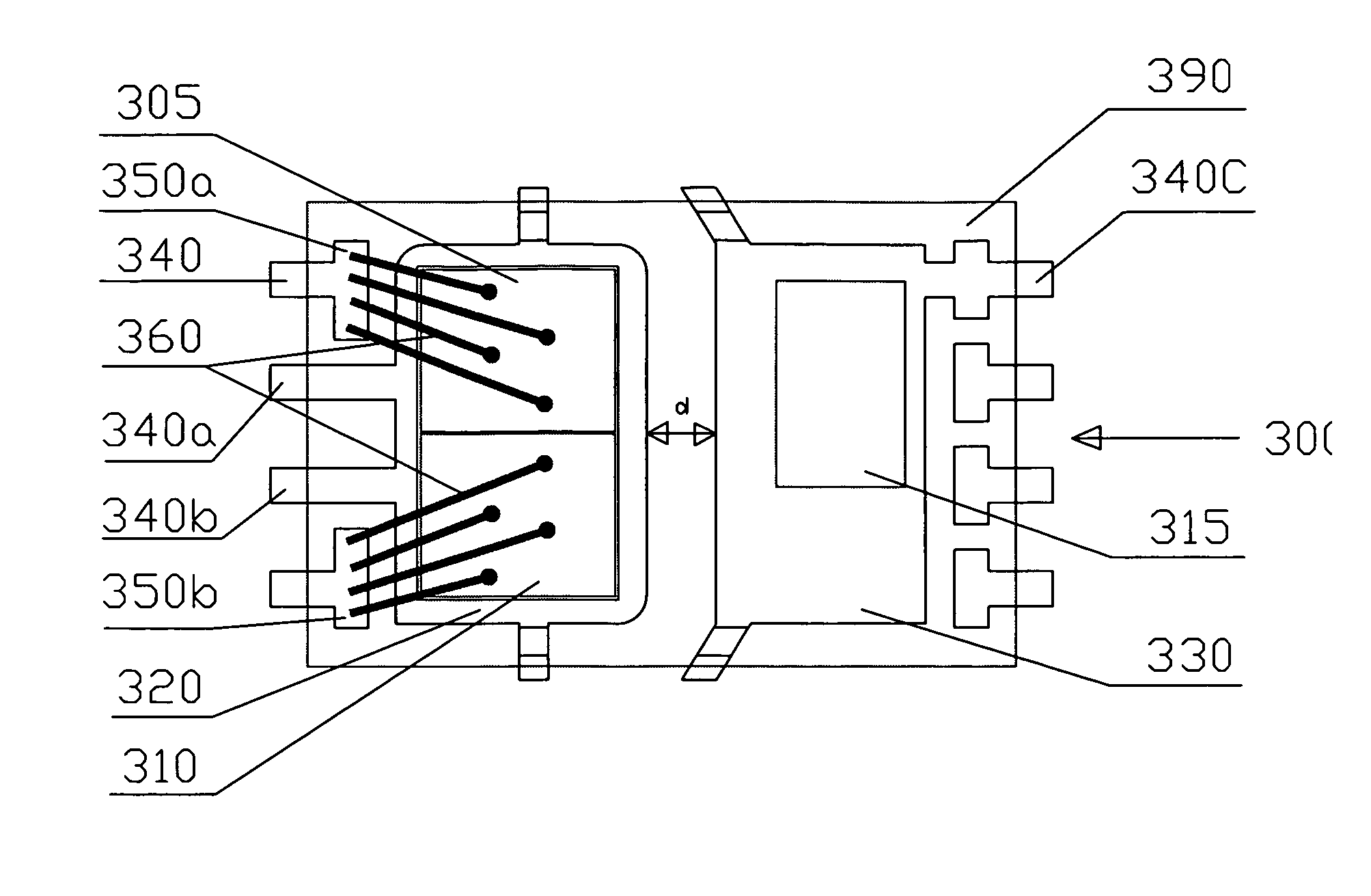
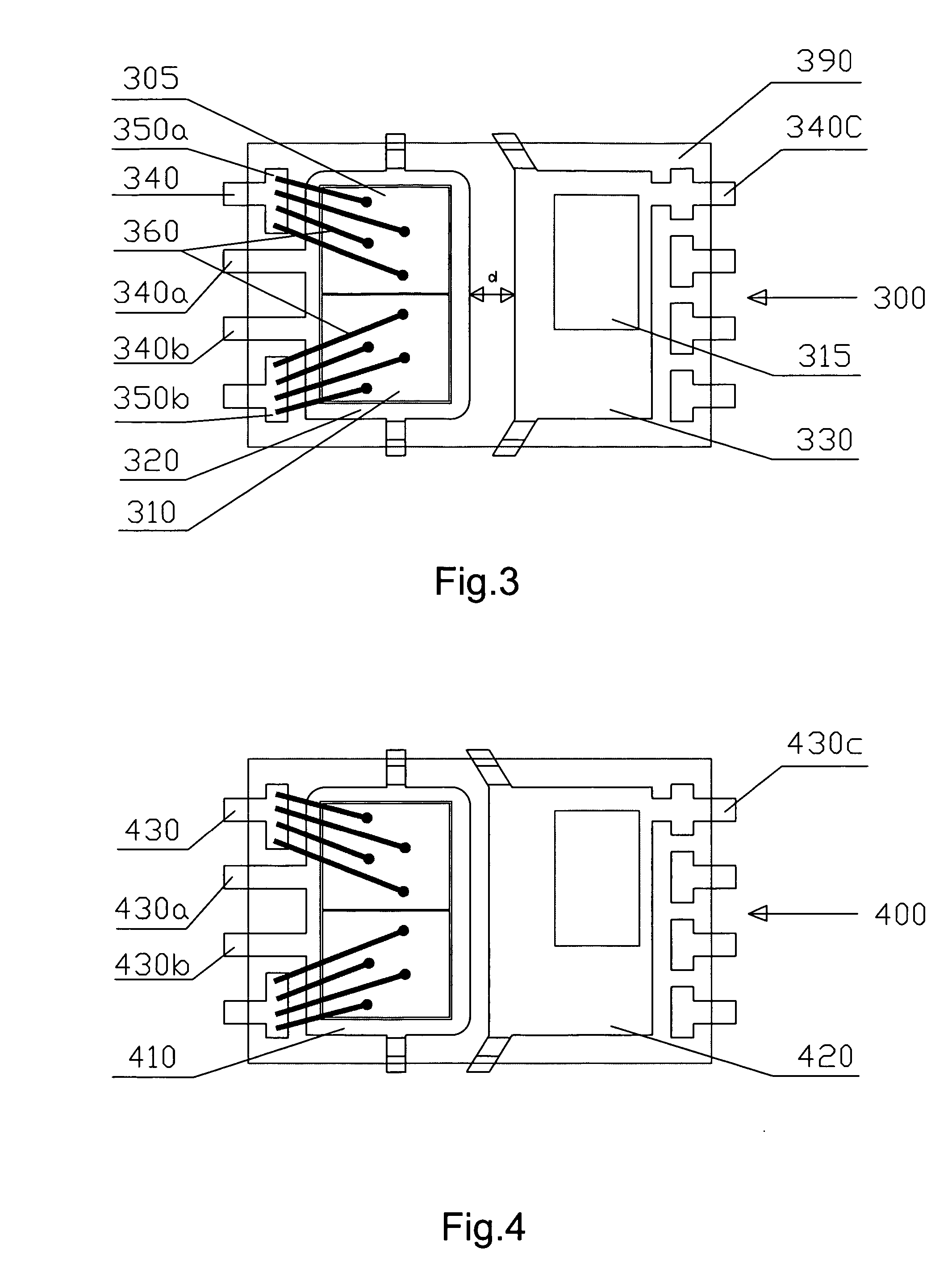
[0020] The present invention discloses a TSSOP-8 semiconductor package having improved thermal performance. The improved thermal performance is achieved by providing a package having first and second lead frame die pads disposed a distance apart from one another to allow for an increased amount of encapsulant therebetween. As the encapsulant includes a material having poor thermal conductivity, the increased amount of encapsulant provides a thermal barrier between common drain MOSFETs and an IC bonded to the first and second lead frame die pads respectively. Additionally, fused leads provide for additional thermal dissipation paths in the package.

[0021] With reference to FIG. 3, a composite TSSOP-8 semiconductor package 300 is shown including a pair of MOSFETs 305 and 310 coupled in a common drain configuration. MOSFETs 305 and 310 may be electrically bonded to a first lead frame die pad 320. An IC 315 may be bonded to a second lead frame die pad 330. Edges of first and second lead ...


PUM


Abstract

A composite semiconductor package is disclosed. The package includes a lead frame having first and second die bonding pads, the first and second die bonding pads having a large lateral separation therebetween, a first device bonded to the first die bonding pad, a second device bonded to the second die bonding pad, a plurality of first leads coupled to the first die bonding pad, a plurality of second leads coupled to the second die bonding pad, and an encapsulant covering the lead frame, the first and second devices and at least a portion of the first and second pluralities of leads. The package may be a TSSOP-8 composite package having a common drain MOSFET pair and an IC.

Description

FIELD OF THE INVENTION [0001] The present invention relates generally to semiconductor packaging and more particularly to a TSSOP-8 semiconductor package including a lead frame design which provides for improved package thermal performance. BACKGROUND OF THE INVENTION [0002] With the increased use of mobile devices such as cellular telecommunication products, portable digital assistants, and tablet PCs, the size, weight and cost of individual electronic components and devices are factors critical to a successful design. Integration of several electronic devices into a single semiconductor package has served this purpose by providing composite or co-packaged devices having the same small package form factor of discreet device packages. [0003] It is known in the art to package a pair of power MOSFETs in a common drain configuration with an integrated circuit (IC) in a TSSOP-8 package. One such package 100 is shown in FIG. 1 and includes a first power MOSFET 105, a second power MOSFET ...

Claims


Application Information

Patent Timeline
IPC IPC(8): H01L23/495
CPCH01L23/49562H01L2924/1306H01L24/49H01L2224/48247H01L2224/48465H01L2224/49111H01L2224/49171H01L2224/49431H01L2924/01015H01L2924/01027H01L2924/01033H01L2924/01074H01L2924/01082H01L2924/13091H01L2924/14H01L24/48H01L2924/01006H01L23/49575H01L2924/00H01L2924/00012H01L2924/00014H01L2224/45099H01L2224/05599
Inventor ZHANG, XIAOTIANCHANG, ARGOLEE, JAMESHUANG, RYANLIU, KAI
Owner ALPHA & OMEGA SEMICON LTD
Why Eureka
Try Eureka