

Light-emitting device
a technology of light-emitting devices and discharge tubes, which is applied in the direction of discharge tubes/lamp details, discharge tubes luminescnet screens, electric discharge lamps, etc., can solve the problems of substantially impossible to extract the light emitted by the device itself, and no means of preventing ambient light from entering the devi
- Summary
- Abstract
- Description
- Claims
- Application Information
AI Technical Summary
Benefits of technology
Problems solved by technology
Method used
Image

Examples
first embodiment
[0022] A light-emitting device of the invention includes a lower electrode, a light-emitting layer, an upper electrode, a protective layer in contact with the upper electrode, and a circular polarizer in contact with the protective layer.
[0023] In other words, the circular polarizer is formed to directly contact the protective layer, and no gap layer or atmospheric layer such as air, gas, or vacuum is present in the device from the circular polarizer to the lower electrode. Since this feature prevents generation of a large refractive index difference within the device, a thin light-emitting device that can prevent ambient light from being emitted from the device is provided.
[0024] The circular polarizer is disposed on the protective layer preferably by using an adhesive so that any irregularities in the protective layer are filled with the adhesive. The thickness of the adhesive preferably corresponds to the depth of the irregularities in the protective layer of the organic light-...
second embodiment
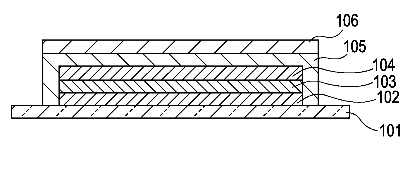
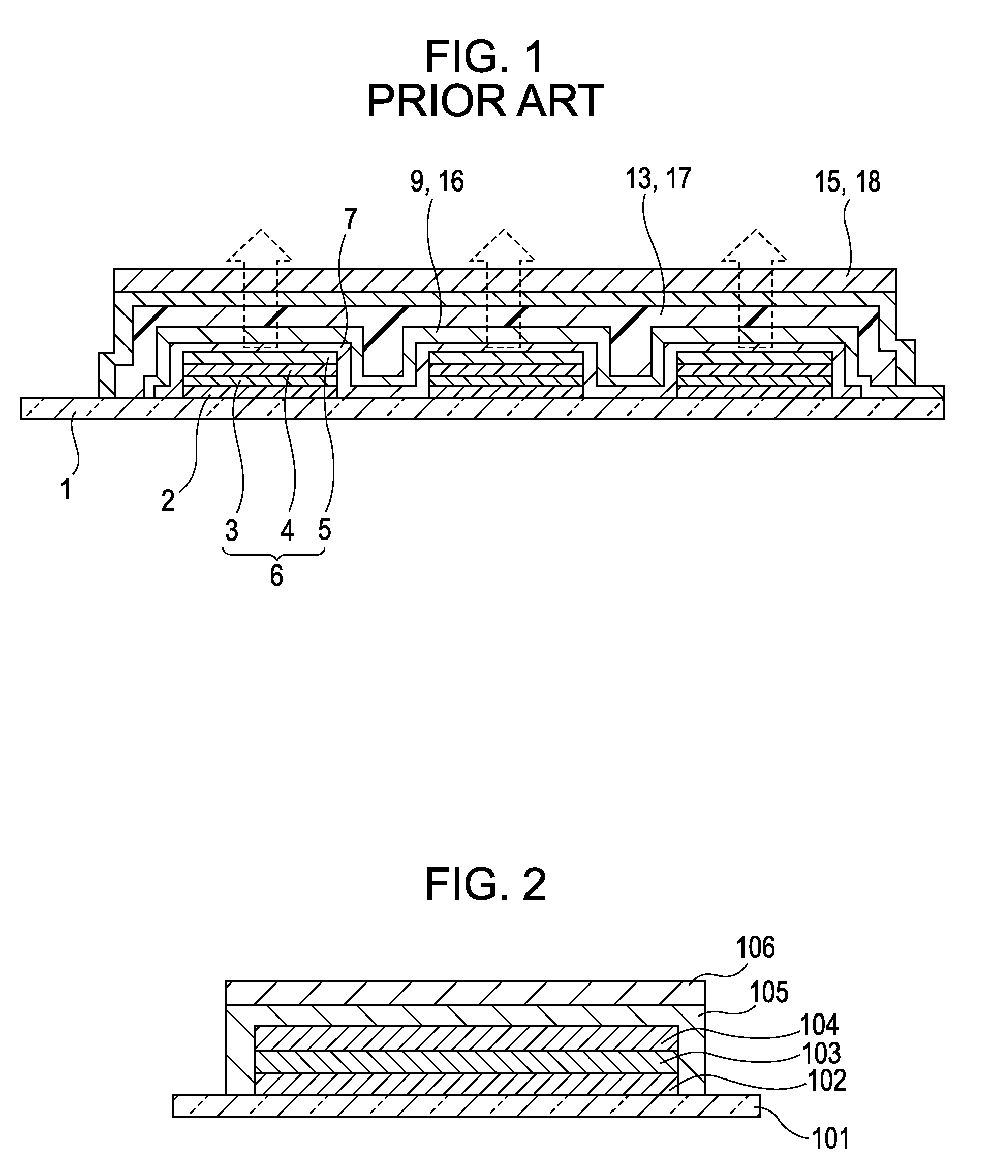
[0033] A light-emitting device according to a first embodiment of the present invention includes a circular polarizer in contact with a protective layer.
[0034]FIG. 2 is a schematic cross-sectional view for explaining the light-emitting device of the first embodiment. Light is extracted in an upward direction.
[0035] The light-emitting device includes a lower electrode 102, a light-emitting layer 103, an upper electrode 104, a protective layer 105, and a circular polarizer 106 sequentially formed on a substrate 101.
[0036] The substrate 101 may be flexible or rigid. An example thereof is a glass substrate. The substrate may be provided with a switching element (not shown) for controlling emission / non-emission. The switching element is, for example, a transistor such as a TFT. When a switching element is provided, the light-emitting device may be disposed on the switching element. In such a case, a planarizing film may be provided between the switching element and the light-emitting ...
example 1
[0063] An organic EL device having a cross-sectional structure shown in FIG. 2 was made as follows.
[0064] First, a TFT circuit and a lower electrode 102 were disposed on a glass substrate having a thickness of 0.7 mm. A light-emitting layer 103, which was a laminated organic EL layer including a hole transport sublayer composed of α-NPD, a light-emitting sublayer composed of Alq3, and a metal-doped sublayer composed of Alq3 doped with an alkali metal, was deposited on the lower electrode 102 by a vapor deposition process. An upper electrode 104 was formed on the layer 103 by sputtering.
[0065] Next, a protective layer 105 composed of SiN was deposited by a CVD process. In the CVD process, a mixed gas containing NH3, SiH4, and N2 was introduced as a material gas into a deposition chamber, and deposition was conducted at a pressure of 100 Pa and a RF power of 100 W. The deposition was terminated when the thickness reached 5,000 Å.
[0066] A circularly polarizing plate 25 μm in thickne...
PUM
 Abstract
Description
Claims
Application Information