Signal processing apparatus for solid-state imaging device, signal processing method, and imaging system

a signal processing and imaging device technology, applied in the direction of color signal processing circuits, television systems, radio frequency controlled devices, etc., can solve the problems of not being able to correct the color mixture with directionality, and not being able to correct the color mixtur

Inactive Publication Date: 2007-06-28
SONY CORP
View PDF2 Cites 218 Cited by
  • Summary
  • Abstract
  • Description
  • Claims
  • Application Information

AI Technical Summary

Benefits of technology

[0015] Since the correction parameters for the signals from the multiple neighboring pixels are independent of each other in the correction of the color mixture between the pixels in the solid-state imaging device, the amount of correction of the color mixture from the neighboring pixels into the target pixel can be arbitrarily set for every neighboring pixel by using the independent correction parameters. As a result, it is possible to give the directionality to the amount of correction of the color mixture from the neighboring pixels into the target pixel, that is, to set different amounts of correction for different neighboring pixels.
[0016] According to the present invention, the directionality can be given to the amount of correction of the color mixture from the neighboring pixels into the target pixel, so that the color mixture can be corrected in accordance with the degree of the color mixture from the neighboring pixels into the target pixel. Consequently, it is possible to realize the correction of the color mixture in accordance with the directionality even if the color mixture from the neighboring pixels into the target pixel has the directionality.

Problems solved by technology

As a result, in related art disclosed in, for example, Japanese Unexamined Patent Application Publication No. 2004-135206, in which the same correction parameter is used for multiple neighboring pixels to correct the color mixture, it is not possible to correct the color mixture in accordance with the degree of the color mixture from the neighboring pixels into the target pixel, that is, it is not possible to correct the color mixture with directionality.

Method used


Image

  • Signal processing apparatus for solid-state imaging device, signal processing method, and imaging system
  • Signal processing apparatus for solid-state imaging device, signal processing method, and imaging system
  • Signal processing apparatus for solid-state imaging device, signal processing method, and imaging system

Examples


first embodiment

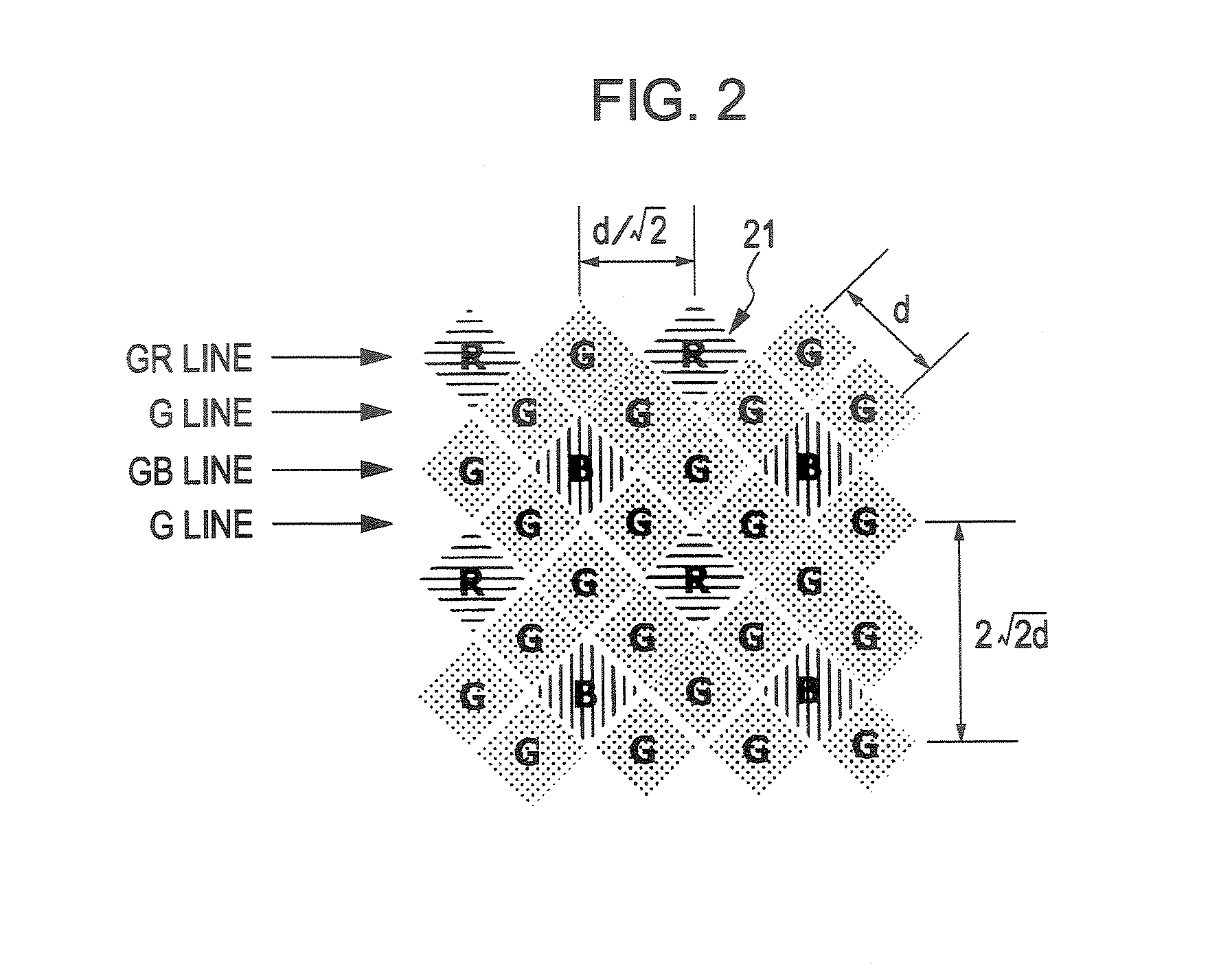
[0076]FIG. 2 shows an example of the color coding of the CMOS image sensor according to a first embodiment of the present invention.

[0077] The CMOS image sensor has a pixel array unit in which pixel cells 21 including the photoelectric transducers are two-dimensionally arranged in an array. As shown in FIG. 2, in the CMOS image sensor according to the first embodiment of the present invention, the pixel cells 21 are arranged at an angle of 45° with respect to the pixel array in a square lattice, typified by the common pixel array in a checker pattern.

[0078] The CMOS image sensor according to the first embodiment of the present invention has pixel shifted arrangement in which the pixels are shifted by half of the pixel pitch √2d for every row and column, where the distance (hereinafter referred to as “pixel pitch”) between the pixels in the pixel array in the square lattice is denoted by “d” and the horizontal and vertical pixel pitch with respect to the pixel pitch “d” is denoted ...

second embodiment

[0183]FIG. 25 is a block diagram schematically showing an example of the structure of a CMOS image sensor 20B according to a second embodiment of the present invention. The same reference numerals are used in FIG. 25 to identify the same components shown in FIG. 3.

[0184] The CMOS image sensor 20B according to the second embodiment has the same pixel arrangement and color coding as those of the CMOS image sensor 20A according to the first embodiment. Specifically, the CMOS image sensor 20B has the color coding, shown in FIG. 2, in which the G components surround the R and B components in the pixel shifted arrangement.

[0185] In the CMOS image sensor 20B, pixel drive lines 23 are wired for every row. The pixel cells 21 in a pixel array unit 22 are selected in units of rows by selection and scanning by a vertical scanning circuit 24 through the pixel drive line 23. Each vertical signal line 25 is commonly wired to the pixel cells 21 in a vertical zigzag column in units of two columns....

third embodiment

[0201]FIG. 32 shows an example of the color coding in a CMOS image sensor according to a third embodiment of the present invention.

[0202] In the CMOS image sensor according to the third embodiment of the present invention, a pixel array unit in which pixel cells including the photoelectric transducers are two-dimensionally arranged in an array has pixel arrangement in a square lattice. The color coding in the pixel arrangement in a square lattice has, for example, a Bayer array shown in FIG. 32.

[0203]FIG. 33 is a block diagram schematically showing an example of the configuration of a CMOS image sensor 20C according to the third embodiment of the present invention. The same reference numerals are used in FIG. 33 to identify the same components shown in FIG. 3.

[0204] Referring to FIG. 33, a pixel array unit 22 has pixel cells 21 including photoelectric transducers, two-dimensionally arranged in a square lattice. In the pixel arrangement in a square lattice, one pixel drive line 23...


PUM


Abstract

A signal processing apparatus corrects color mixture between pixel cells in a solid-state imaging device in which the pixel cells including photoelectric transducers are two-dimensionally arranged in an array and in which color filters having primary color components for generating luminance components and other color components are arranged over the pixel cells. The signal processing apparatus includes correction processing means for performing the correction to the signal from a target pixel by using the signals from multiple neighboring pixels adjacent to the target pixel in the solid-state imaging device and correction parameters independently set for the signals.

Description

CROSS REFERENCES TO RELATED APPLICATIONS [0001] The present invention contains subject matter related to Japanese Patent Application JP 2005-332308 filed in the Japanese Patent Office on Nov. 17, 2005, the entire contents of which are incorporated herein by reference. BACKGROUND OF THE INVENTION [0002] 1. Field of the Invention [0003] The present invention relates to signal processing apparatuses for solid-state imaging devices, signal processing methods, and imaging systems. More particularly, the present invention relates to a signal processing apparatus capable of correcting color mixture in the pixel area of a solid-state imaging device, a signal processing method in the signal processing apparatus, and an imaging system including the signal processing apparatus. [0004] 2. Description of the Related Art [0005] Solid-state imaging devices, such as charge coupled device (CCD) image sensors and complementary metal oxide semiconductor (CMOS) image sensors, have structures in which c...

Claims


Application Information

Patent Timeline
Patent Type & Authority Applications(United States)
IPC IPC(8): H04N9/04H01L27/146H04N9/07
CPCH04N5/335H04N9/045H04N25/00H04N23/84H04N25/134
Inventor KINOSHITA, MASAYAUNE, HIDEHOTANAKA, MASAHITO
Owner SONY CORP
Why Eureka
Try Eureka