


Quick Research
Generate reliable direction feasibility study reports for your R&D in just a few steps.

Technical Q&A
Discover and master advanced knowledge NOW. Basics, ideas, possibilities, all at once.

Find Solutions
As an expert in R&D theories, this can generate solutions to your technical problems instantly.

Evaluate Feasibility
Analyze your overall solution with one click, know your potential R&D risks in advance.

Monitor Landscape
Get weekly tech updates, stay abreast of the latest tech innovations and key insights.
Devices and methods for controlling active termination resistors in a memory system
- Summary
- Abstract
- Description
- Claims
- Application Information
AI Technical Summary
Benefits of technology
Problems solved by technology
Method used
Image

Examples
second embodiment
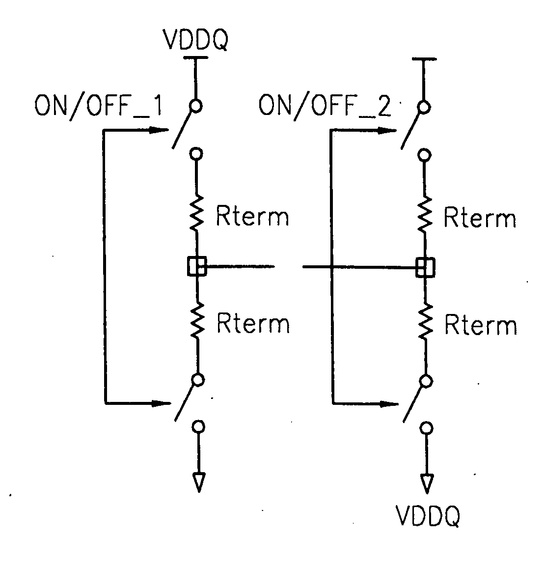
[0070] the present invention will now be described with initial reference to FIG. 11 of the drawings. In this embodiment, DRAM chips positioned on each side of each DiMM module are individually ATC controlled by the combination of common ATC signaling and mode registers. In particular, as shown in FIG. 11, the memory system 1100 includes a chipset 1110, a data bus 1120, a first memory module 1140 in which DRAMs 1160 and 1170 are mounted, and a second memory module 1150 in which DRAMs 1180 and 1190 are mounted. The memory modules 1140 and 1150 may be mounted in card slots (not shown) of the memory system 1100.
[0071] The first and second memory modules 1140 and 1150 may be implemented, for example, by a dual in-line memory module (DiMM). Further, while two DRAMs 1160 (1180) and 1170 (1190) are illustrated in FIG. 11 for each of the modules 1140 and 1150, additional DRAMs may be mounted in each of the first and second memory modules 1140 and 1150. Also, each of the chipset 1110 and the...
first embodiment
[0072] In contrast to the first embodiment, the DRAMs 1160, 1170, 1180 and 1190 are additionally equipped with a mode register 1105 which includes data indicative of the operational mode (active, power down, standby) of a corresponding DRAM. In a manner described below with reference to FIGS. 12A through 12E, the output of each register controls the operation of the MUX 604 of each ATC control circuit shown in FIG. 6 to thereby select a synchronous or asynchronous control mode.
[0073]FIG. 13 illustrates a “2r / 2r” configuration in which each of the first and second memory modules DiMM0 and DiMM1 are equipped with two DRAM circuits. In this case, the active terminator control (ATC) of the memory system is carried out as shown below in FIG. 12A. Here, Rank 0 (R0) designates DRAM 1160, Rank 1 (R1) designates DRAM 1170, Rank 2 (R2) designates DRAM 1180, and Rank 3 (R3) designates DRAM 1190.
[0074] In FIG. 12A, “Off(flag)” means that the termination resistors are disabled exclusively by th...
third embodiment
[0080] the present invention will now be described with reference to FIG. 18 of the drawings. In this embodiment, DRAM chips 1860 (1880) and 1870 (1890) positioned on each side of each of the memory modules DiMM are individually ATC controlled by individual ATC signals issued from the chipset. In particular, as shown in FIG. 18, the memory system 1800 includes a chipset 1810, a data bus 1820, a first memory module 1840 in which DRAMs 1860 and 1870 are mounted, and a second memory module 1850 in which DRAMs 1880 and 1890 are mounted. The memory modules 1840 and 1850 may be mounted in card slots (not shown) of the memory system 1800.
[0081] The first and second memory modules 1840 and 1850 may be implemented, for example, by a dual in-line memory module (DiMM). Further, while two DRAMs 1860 (1880) and 1870 (1890) are illustrated in FIG. 18 for each of the modules 1840 and 1850, additional DRAMs may be mounted in each of the first and second memory modules 1840 and 1850. Also, each of t...
PUM
 Abstract
Description
Claims
Application Information
 - R&D Engineer
- R&D Manager
- IP Professional
- Industry Leading Data Capabilities
- Powerful AI technology
- Patent DNA Extraction
Browse by: Latest US Patents, China's latest patents, Technical Efficacy Thesaurus, Application Domain, Technology Topic, Popular Technical Reports.
© 2024 PatSnap. All rights reserved.Legal|Privacy policy|Modern Slavery Act Transparency Statement|Sitemap|About US| Contact US: help@patsnap.com