Write burst stop function in low power DDR sDRAM

Inactive Publication Date: 2007-06-28
POLARIS INNOVATIONS
View PDF4 Cites 7 Cited by
  • Summary
  • Abstract
  • Description
  • Claims
  • Application Information

AI Technical Summary

Problems solved by technology

An undesirable alternative to interrupting the write bu

Method used


Image

  • Write burst stop function in low power DDR sDRAM
  • Write burst stop function in low power DDR sDRAM
  • Write burst stop function in low power DDR sDRAM

Examples


Embodiment Construction

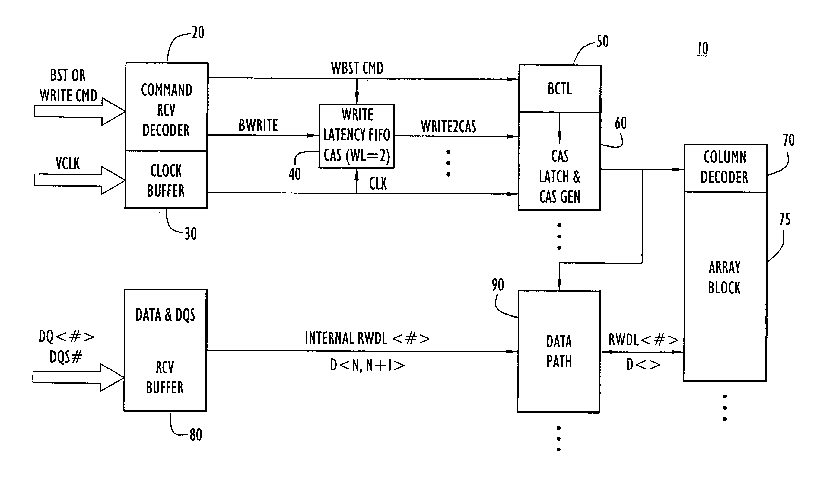
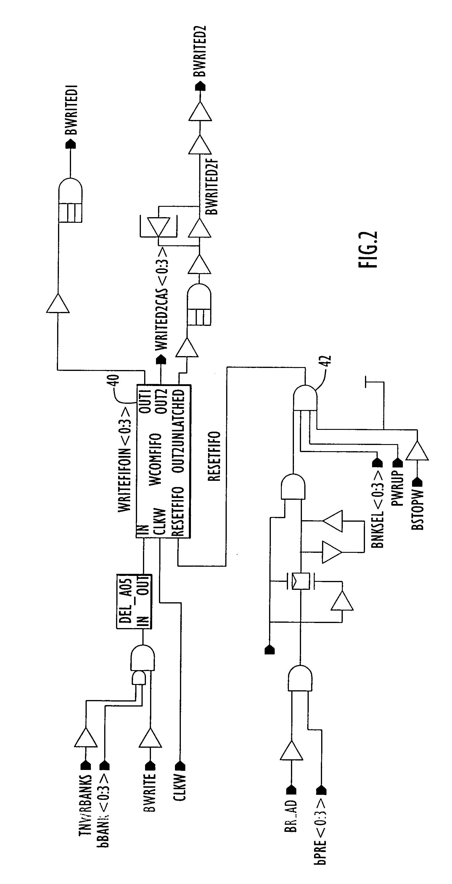
[0011] Referring first to FIG. 1, the circuitry in a semiconductor memory device 10 that is relevant to the write burst stop function is shown. There is a command receive decoder 20 that receives command signals from a host device (not shown) including, in particular, a write command (WRITE CMD) signal and a burst stop command (BST) signal. There is also a clock buffer circuit 30 that receives a clock signal (VCLK) supplied by the host device. The command receive decoder 20 is connected to a write latency first-in first-out (FIFO) circuit 40 and to a burst control circuit (BCTL) 50. The clock buffer 30 is also connected to the write latency FIFO 40 and to a column address strobe (CAS) latch and CAS generator circuit 60. The CAS latch and CAS generator circuit 60 is connected to a column decoder 70 and memory cell array 75 for a memory bank. The memory device 10 may have multiple memory banks and the circuits 40 and 60 are repeated for the memory array of each bank.

[0012] Data recei...


PUM


Abstract

A write burst stop command function is provided for a semiconductor memory device, and in particular for a memory device having a write latency, such as is common in a low power double data rate (DDR) dynamic random access memory (DRAM) device. In the memory device, when a write stop command is received, pulses that are generated for a column address strobe signal are terminated so that no further data already in the memory device is transferred into a memory array. When the write stop command is received at the beginning of a write operation prior to generation of the pulses in the column address strobe signal, a first-in first-out (FIFO) circuit is reset. The FIFO circuit is used to introduce a predetermined write latency to the write operation. The column address strobe signal is supplied to a column decoder associated with the memory array and to a data path circuit that transfers data to the memory array based on pulses in the column address strobe signal. In one embodiment, the pulses for the column address strobe signal are produced by a latch circuit based on a signal derived from the output of the write latency FIFO circuit and so an input to the latch is disabled in response to the write stop command to stop producing pulses for the column address strobe signal.

Description

BACKGROUND OF THE INVENTION [0001] The present invention is directed to semiconductor devices, and more particularly to stopping a write burst function in a semiconductor integrated circuit memory device, such as a low power double data rate (DDR) dynamic random access memory (DRAM) device. [0002] In certain semiconductor memory devices, such as DRAM devices designed for lower power consumption applications, such as portable computing devices (laptops, PDAs, etc.), the length (amount of data) of a write burst is longer than commodity DRAMs designed for less restricted power applications. These types of write burst operations are also called full page bursts. [0003] The host device may need to stop the write burst due to host device application requirements. For example, a host device application may need to urgently read out data and must interrupt an ongoing write burst to do so. An undesirable alternative to interrupting the write burst is to close the memory array with a precharg...

Claims


Application Information

Patent Timeline
IPC IPC(8): G11C7/00
CPCG11C7/1027G11C7/1066G11C7/1078G11C7/109G11C11/4076G11C11/4093
Inventor SCHNELL, JOSEFFREEBERN, MEG
Owner POLARIS INNOVATIONS
Why Eureka
Try Eureka