Method for Manufacturing CMOS image sensor
- Summary
- Abstract
- Description
- Claims
- Application Information
AI Technical Summary
Benefits of technology
Problems solved by technology
Method used
Image
Examples
Embodiment Construction
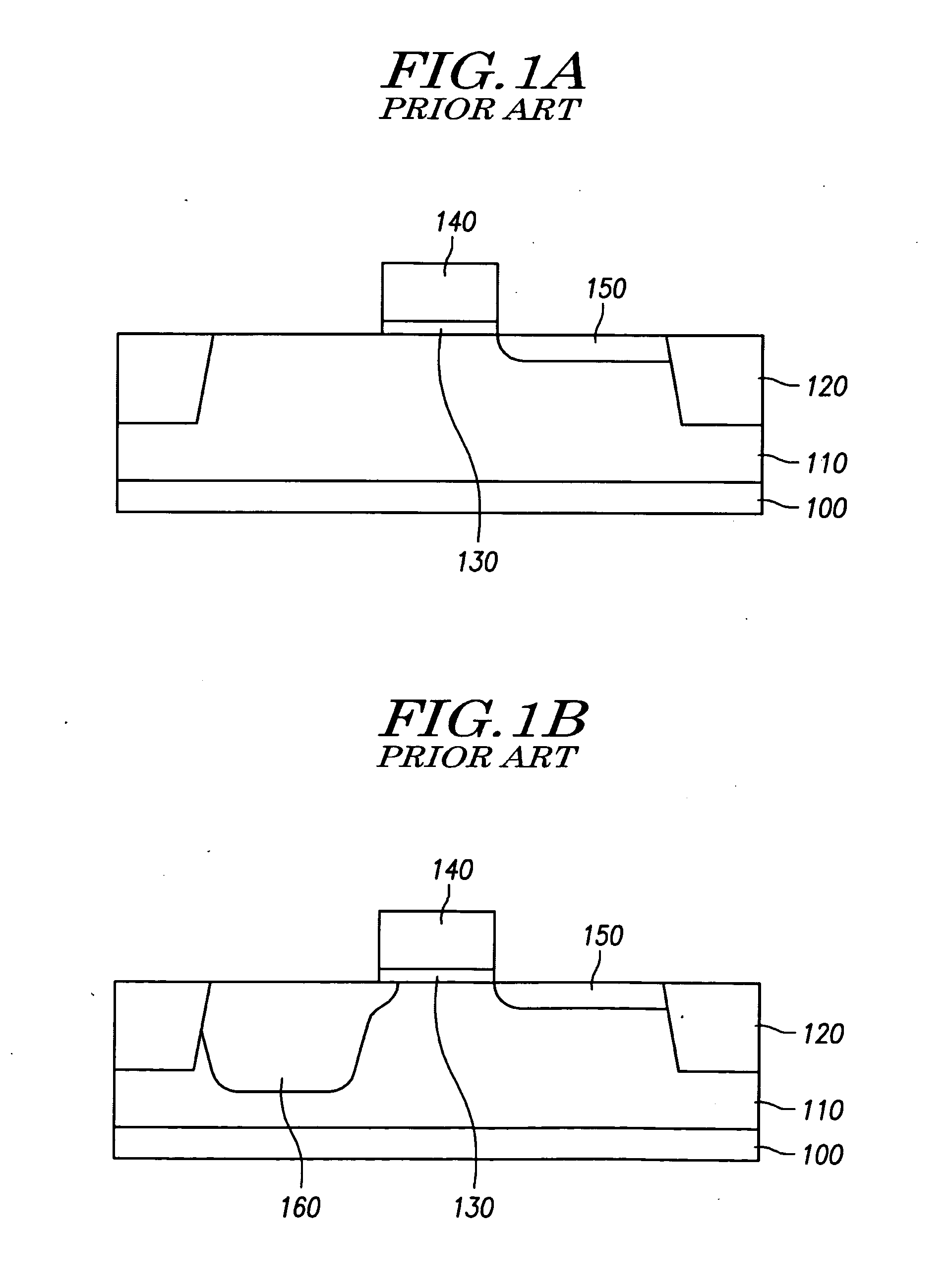
[0024] Hereinafter, a method for manufacturing a CMOS image sensor according to the present invention will be described in detail with reference to accompanying drawings.
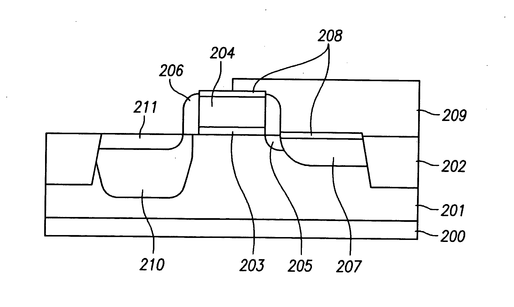
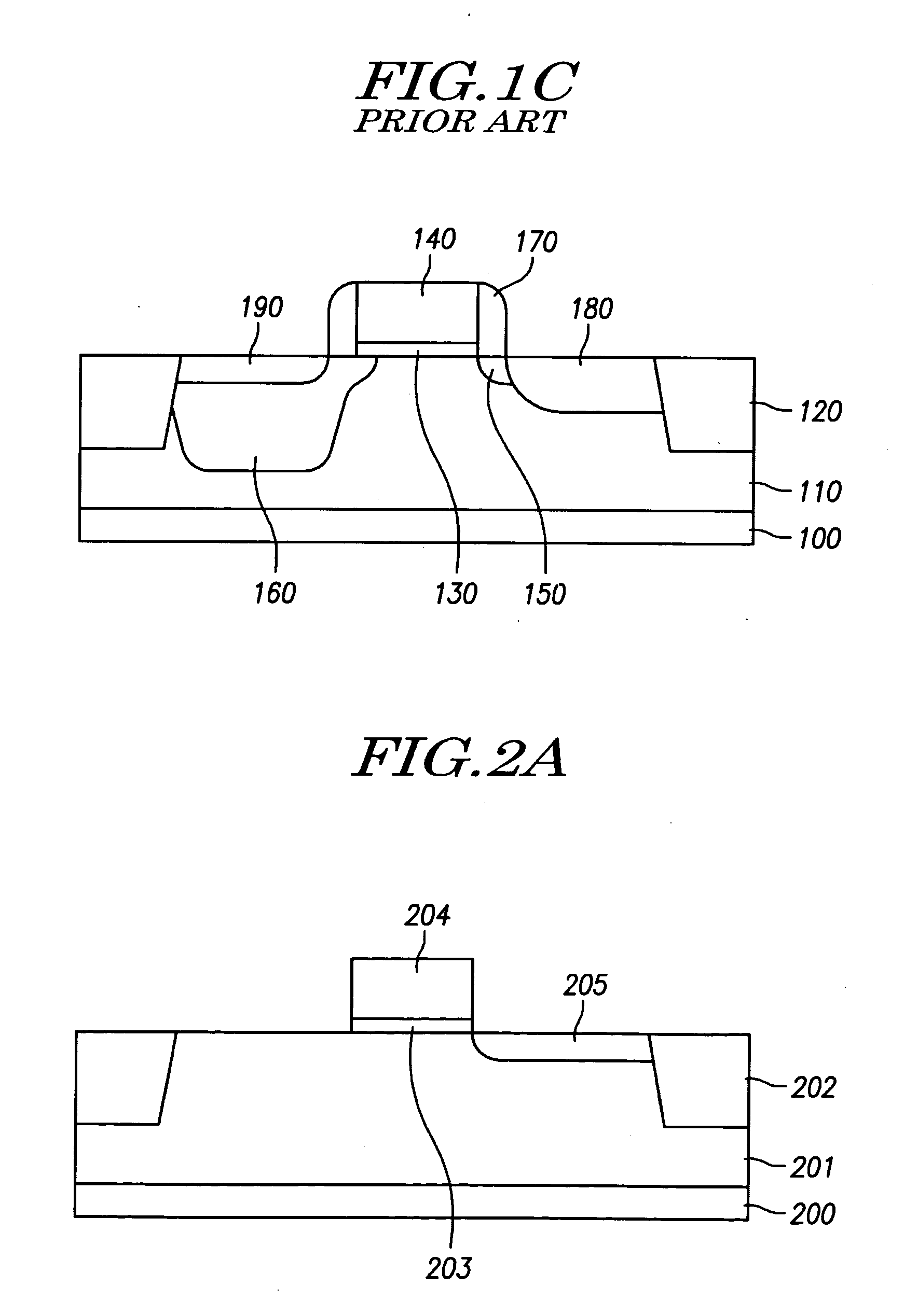
[0025]FIGS. 2A to 2C are sectional views showing a CMOS image sensor according to an embodiment of the present invention.
[0026] As shown in FIG. 2A, a low-density P type (P-) epitaxial layer 201 is formed on a P type semiconductor substrate 200. Then, a photoresist film (not shown) is coated on the epitaxial layer 201. Thereafter, an exposure and development process is performed with respect to the photoresist film by using a mask defining an active area and an isolation area, thereby forming a photoresist pattern such that only a portion of the epitaxial layer 201 corresponding to the isolation area is exposed. The exposed epitaxial layer 201 is etched by a predetermined depth by using the photoresist pattern as a mask, thereby forming a trench (not shown). Thereafter, the photoresist pattern is removed.
[0027] S...
PUM
 Abstract
Description
Claims
Application Information


