
Memory packaging structure of mini SD card

Inactive Publication Date: 2007-07-12
ADATA +1
View PDF3 Cites 14 Cited by
  • Summary
  • Abstract
  • Description
  • Claims
  • Application Information

AI Technical Summary

Benefits of technology

[0006]The main purpose of the present invention is to provide a memory which itself is packaged by TSOP, and which, after special processes such as pin adjustment, can be placed into a general mini SD card, substituting the complicated and non-economical memory packaging structure currently used, allowing the production cost of mini SD card to become less by means of reduction of internal memory component cost.
[0007]Another purpose of the present invention is to expand the memory capacity by means of applying TSOP packaging structure to memory in the mini SD card, such that the memory capacity of mini SD card becomes bigger, enabling the users of mini SD save expenditure on purchasing extra memory cards, enhancing thus market competitiveness.
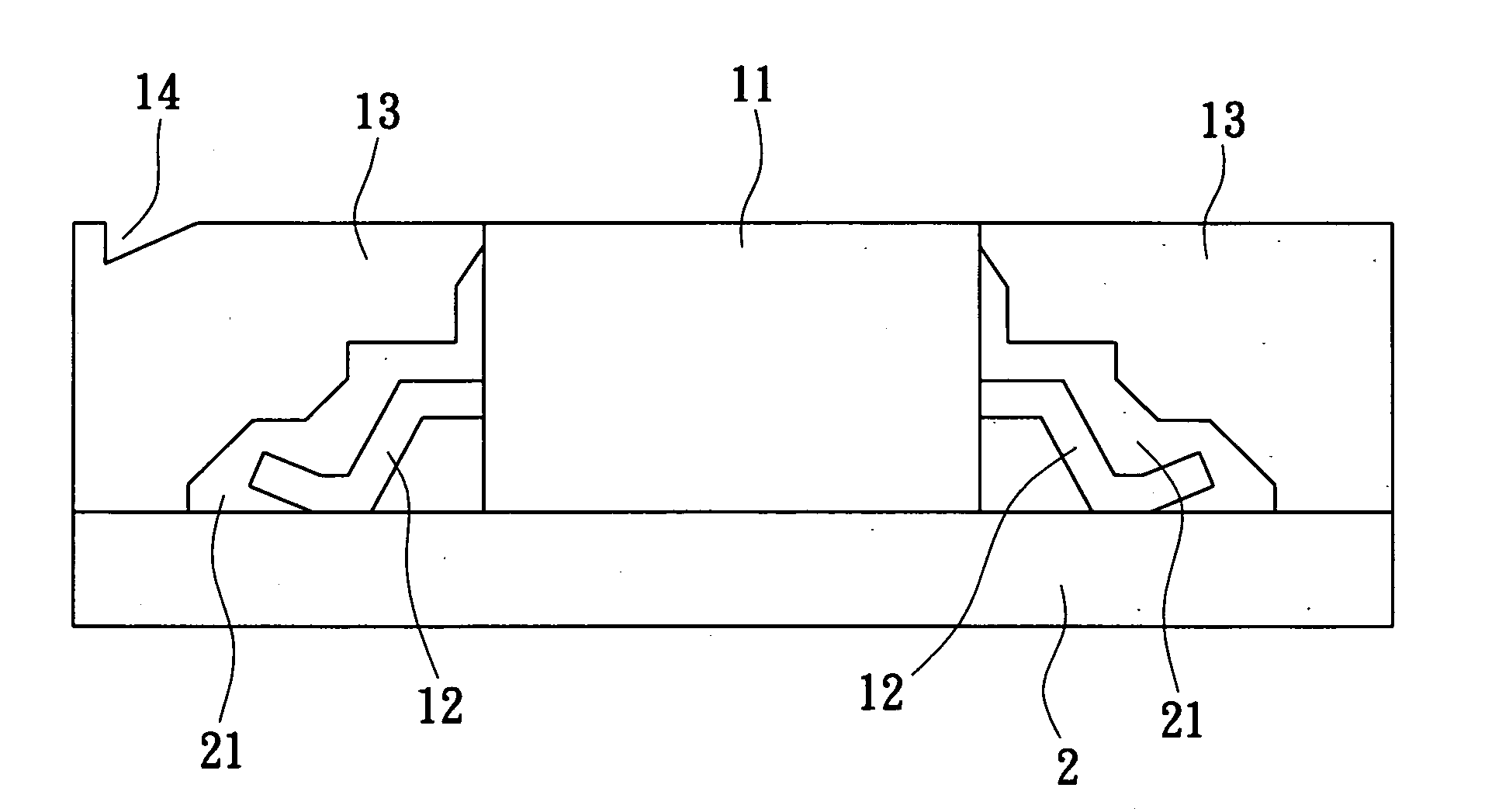
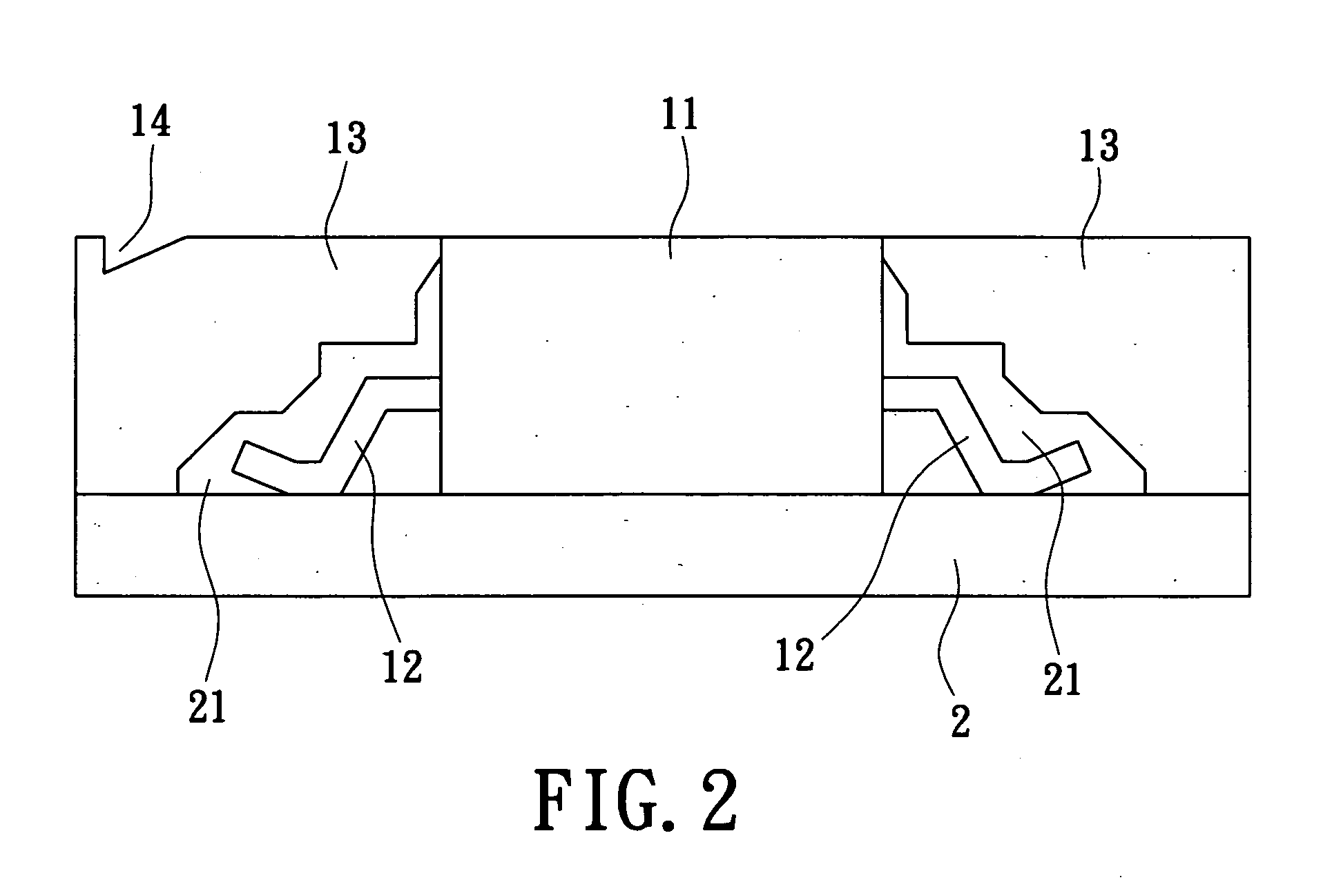
[0008]Accordingly, the principal technical means of the present invention is to perform pin adjustment to the pins on both sides of the memory fabricated in accordance with TSOP packaging structure, such that the existing gaps between the memory and the circuit board can hence be totally eliminated, pushing the memory lower thus completely attached to the surface on lower layer circuit board; while the top end of the memory being open without any coverage, allowing the mini SD card to reduce the thickness of auxiliary lateral body required for sealing the top end of the memory, then covering (sealing) the pins on both sides of the memory to the height aligned with the memory, in which the gaps between pins and auxiliary lateral bodies can be glued to enhance the attachment, achieving the effect of memory fixation assistance.

Problems solved by technology

Memories employing different packaging technologies also create significant differences in performance.
Not hard to see that such package size is larger than chip, illustrating its low packaging efficiency, taking up much effective packaging area.
Aforementioned universal packaging structure can reduce the thickness of memory packages, but package procedures thereof are more complicated and cost more, more susceptible to flaws and hence increasing production overhead, which, compared with TSOP packaging structure used inside SDRAM, represents a type of less economical packaging structure.

Method used


Image

  • Memory packaging structure of mini SD card
  • Memory packaging structure of mini SD card
  • Memory packaging structure of mini SD card

Examples


Embodiment Construction

[0014]Hereunder the implementations of the present invention will be further discussed with reference to appended drawings and component symbols, enabling the ones skilled in the art being able to practice the present invention upon reading the specification document.

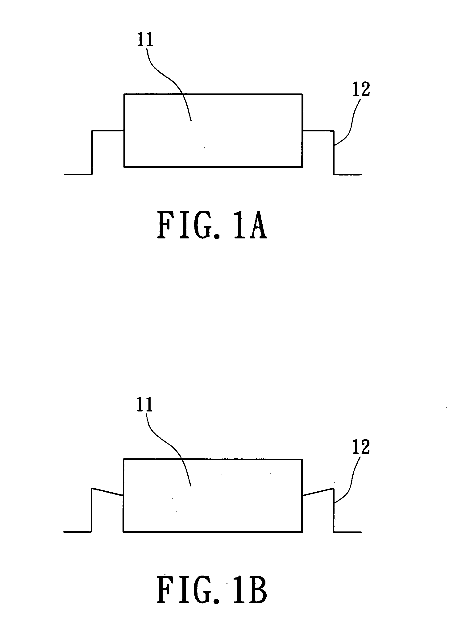
[0015]Now refer to FIG. 1, wherein shows a side view diagram of the memory employing TSOP packaging structure. FIG. 1a illustrates a normal TSOP pin connection condition, in which the pin 12 extends from the two sides of the memory 11 and turns downward after a right angle, allowing the pin to support the memory 12 up and to create a gap of 0.2 mm from the surface of printed circuit board. To make the best of the internal space of a mini SD card, allowing the memory 11 utilizing TSOP packaging structure to be placed inside the board with limited space, it is required to perform pin adjustment such that the memory can be completely attached to printed circuit board, as the pin connection condition shown in FIG. 1b. After...


PUM


Abstract

A memory packaging structure of mini SD card, the main implementation technology thereof comprises: to perform the pin adjustment to the: memory originally employing TSOP (Thin Small Out-Line Package) packaging structure, eliminating the gap of 0.1 mm to 0.2 mm between the memory and the circuit board, thus completely attached to the circuit board; to leave the top end of the mini SD card open to directly expose the top end of the memory on the surface of the mini SD card, reducing the thickness of a layer of coverage; to cover the pins on the both sides of the memory to hind them, wherein applying glue joint between the auxiliary lateral body and memory pins to enhance the attachment.

Description

BACKGROUND OF THE INVENTION[0001]1. Field of the Invention[0002]The present invention relates to a memory packaging structure of mini SD card, in particular to a packaging structure of TSOP (Thin Small Out-Line Package) memory.[0003]2. Background of the Invention[0004]In order to integrally accelerate the computer process speed, the entire system thereof needs to be enhanced, while memory has always been another focus of attention, whose technology of fabrication similarly determines the performance thereof, and the packaging technology stands for one critical stage in the memory fabrication workflow. Memories employing different packaging technologies also create significant differences in performance. From DIP, TSOP to BGA, continuous development of packaging technology enables memory stride toward goals of high frequency and high speed, and the emergence of new technologies, such as CSP, symbolizes that memory packaging has now entered the CSP era. Each bar of memory used nowaday...

Claims


Application Information

Patent Timeline
IPC IPC(8): H01L23/02
CPCH01L23/3107H05K3/284H01L2924/1815H01L2924/0002H01L2924/00
Inventor CHUANG, PING-YANG
Owner ADATA
Learn More