Conductive structures for electrically conductive pads of circuit board and fabrication method thereof

a technology of electrically conductive pads and conductive structures, which is applied in the direction of resist details, printed circuit aspects, printed circuit manufacturing, etc., can solve the problems of adversely affecting the electrical connection between the chip and the circuit board, and difficult control of the height of solder bumps or solder balls in the subsequent process, so as to prevent metal interface problems, fine electrical conductive, and the effect of overcoming

Active Publication Date: 2007-07-12
PHOENIX PRECISION TECH CORP
View PDF10 Cites 25 Cited by
  • Summary
  • Abstract
  • Description
  • Claims
  • Application Information

AI Technical Summary

Benefits of technology

[0015]According to another embodiment of the present invention, the first connecting layer on the metal layer of the second electrically conductive pads can be removed first and then the second connecting layer is formed on the metal layer, thereby keeping the composition stability of the second connecting layer and meanwhile preventing metal interface problem between the first and second connecting layers.
[0016]Therefore, a metal layer and a first connecting layer are formed on the first electrically conductive pads; a metal layer, a first connecting layer and a second connecting layer are formed on the second electrically conductive pads; and a metal layer and a first connecting layer are formed on the third electrically conductive pads. In addition, conductive structures can be directly formed on the electrically conductive pads without the need of forming the metal layer, thereby meeting practical need for dif...

Problems solved by technology

As a result, solder bumps and surface mounting component conductive structures exist on the circuit board at the same time.
However, in the stencil printing process, the higher the solder materials, the more difficult it is to control the height of solder bumps or solder balls in subsequent process.
Thereby, solder bumps or solder balls of uneven heights are formed in the reflow process, which adversely affects the electrical connection between the chi...

Method used


Image

  • Conductive structures for electrically conductive pads of circuit board and fabrication method thereof
  • Conductive structures for electrically conductive pads of circuit board and fabrication method thereof
  • Conductive structures for electrically conductive pads of circuit board and fabrication method thereof

Examples


first embodiment

[0022]FIGS. 2A to 2I show a fabrication method of conductive structures for electrically conductive pads of a circuit board according to a first embodiment of the present invention.

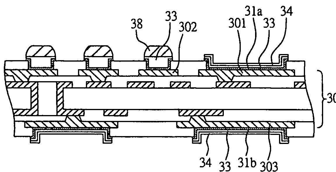
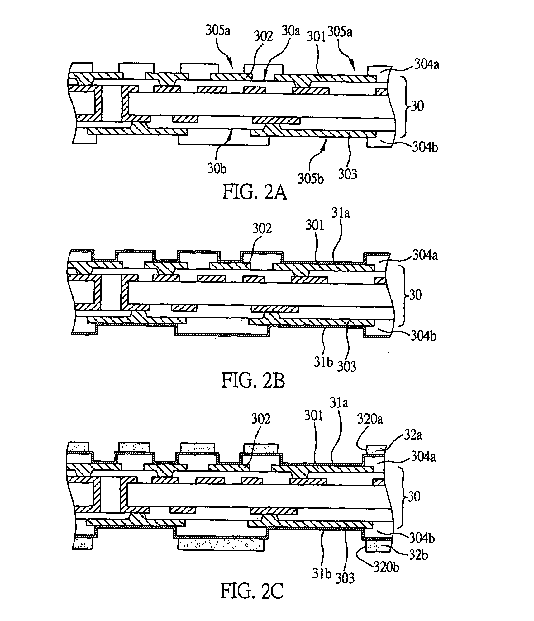
[0023]Referring to FIG. 2A, a circuit board 30 having a first surface 30a and a second surface 30b is provided. On the first surface 30a of the circuit board 30, there is formed a plurality of first electrically conductive pads 301 and second electrically conductive pads 302 of different size. On the second surface 30b of the circuit board 30, there is formed a plurality of third electrically conductive pads 303. A first and a second insulating protection layers 304a, 304b are respectively formed on the first and second surfaces 30a, 30b of the circuit board 30, and a plurality of openings 305a, 305b is respectively formed in the first and second insulating protection layers 304a, 304b by a patterning process such as exposure and development so as to expose the first, second and third electrically conduct...

second embodiment

[0034]FIGS. 3A to 3D show a fabrication method of conductive structures for electrically conductive pads of a circuit board according to a second embodiment of the present invention. Difference of the present embodiment from the first embodiment is the second connecting layer is formed after the first connecting layer on the metal layer of the second electrically conductive pads is removed. The detailed process is described as follows.

[0035]As shown in FIG. 3A, as a succession of the fabrication process in FIG. 2F of the first embodiment, the first connecting layer 34 on the metal layer 33 in the opening 350a of the third resist layer 35a is removed by etching or electrolyzing.

[0036]As shown in FIG. 3B, the second connecting layer 36 is formed on the metal layer 33 in the opening 350a of the third resist layer 35a.

[0037]As shown in FIG. 3C, the third, fourth resist layers 35a, 35b and the first, second resist layers 32a, 32b are removed, and the first, second conductive layers 31a,...


PUM

PropertyMeasurementUnit
Electrical conductivityaaaaaaaaaa
Adhesion strengthaaaaaaaaaa
Electrical conductoraaaaaaaaaa

Abstract

Conductive structures for electrically conductive pads of a circuit board and fabrication method thereof are proposed. The fabrication method includes: providing a circuit board with a plurality of first, second and third electrically conductive pads; forming first and second conductive layers on the circuit board; forming first and second resist layers respectively on the first and second conductive layers, the resist layers having a plurality of openings for exposing the conductive layers on the pads; forming a metal layer in the openings of the first and second resist layers; and forming a first connecting layer on the metal layer; forming third and fourth resist layers on the first and second resist layers respectively, the third resist layer having a plurality of openings for exposing the first connecting layer on the metal layer on the second electrically

Description

BACKGROUND OF THE INVENTION[0001]1. Field of the Invention[0002]The present invention relates generally to conductive structures for electrically conductive pads of a circuit board and fabrication method thereof, and more particularly to a fabrication method of different conductive structures for electrically conductive pads on surface of a circuit board for different electronic component connections.[0003]2. Description of Related Art[0004]In a flip chip package, a plurality of electrode pads is disposed on surface of an IC chip and a plurality of solder bumps is formed on the electrode pads. Corresponding to the electrode pads and the solder bumps, a plurality of electrically conductive pads and solder bumps is formed on an organic circuit board such that the IC chip can be disposed on the packaging substrate with its active surface facing down.[0005]Due to increasing demands for electronic products having high speed, high functionality and small size, application field of the fli...

Claims


Application Information

Patent Timeline
IPC IPC(8): H01L21/44
CPCH05K3/243H05K3/3473H05K3/4007H05K3/4644H05K2201/0367H05K2201/0391Y10T29/49165H05K2201/09472H05K2201/09509H05K2201/09563H05K2203/043H05K2203/054H05K2203/0574H05K2201/09436
Inventor HU, WEN-HUNGWANG, YING-TUNGHSU, SHIH-PINGSHIH, CHAO-WEN
Owner PHOENIX PRECISION TECH CORP
Why Eureka
Try Eureka