Droplet ejection head driving circuit and method, and droplet ejection device
- Summary
- Abstract
- Description
- Claims
- Application Information
AI Technical Summary
Benefits of technology
Problems solved by technology
Method used
Image
Examples
first exemplary embodiment
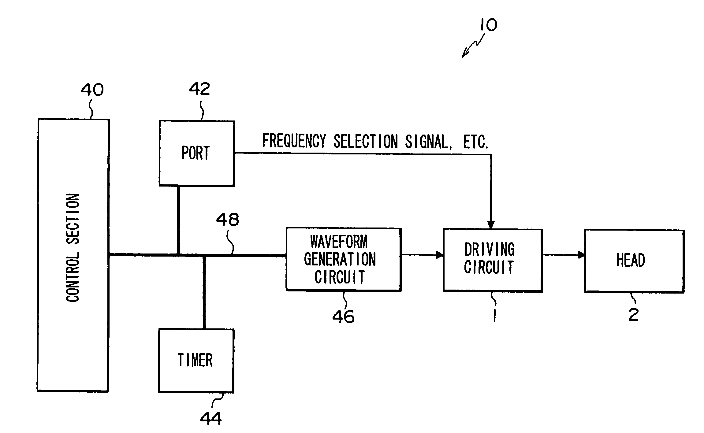
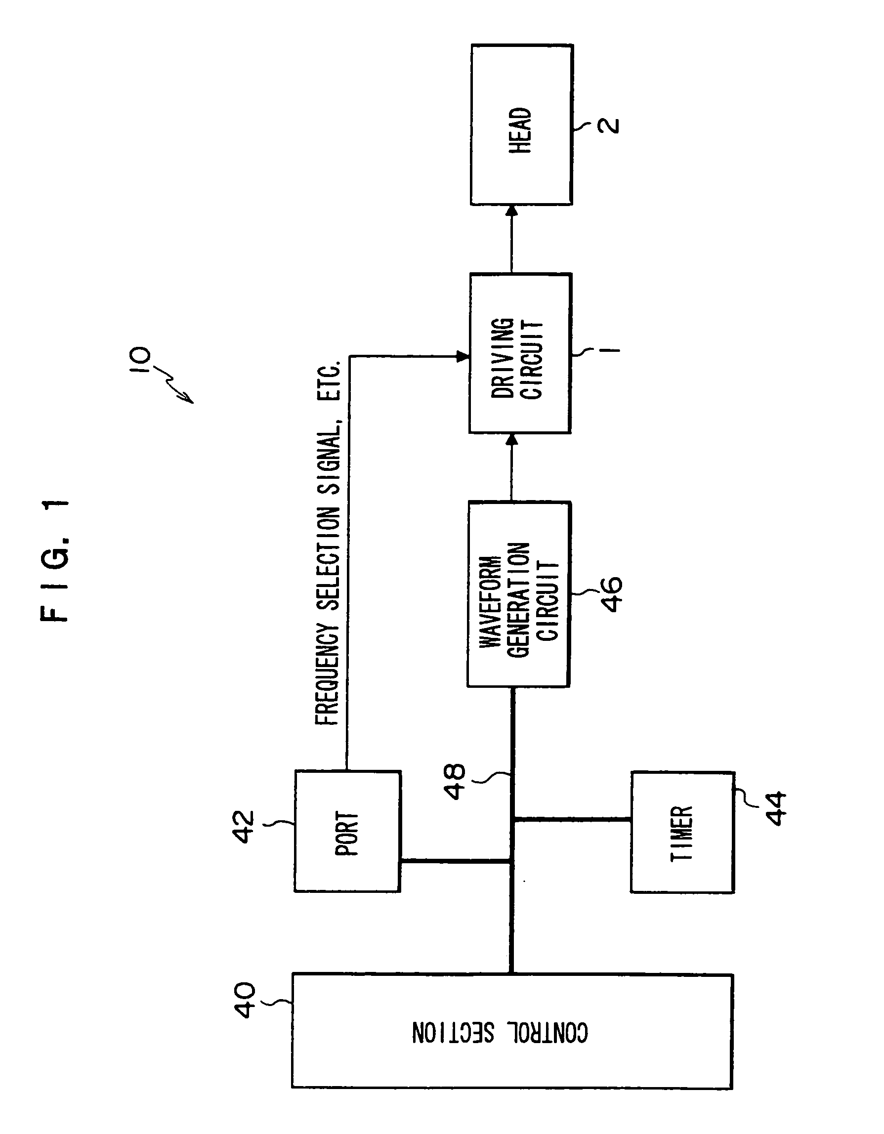
[0027]FIG. 1 shows a schematic block diagram of a control system of a droplet ejection device 10. As shown in FIG. 1, the droplet ejection device 10 is structured with a driving circuit 1, a head 2, a control section 40, a port 42, a timer 44 and a waveform generation circuit 46. The control section 40, port 42, timer 44 and waveform generation circuit 46 are connected via a bus 48.
[0028]The droplet ejection device 10 operates in respective modes of a preliminary state (warm-up), an operation state (running), a waiting state (stand-by), and a paused state (sleep). The warm-up state is a state in which, for example, initialization processing and the like for an unillustrated memory, logic circuit and the like of the droplet ejection device 10 is executed. The running state is a state during execution of printing in accordance with inputted printing data. The standby state is a state from which is possible to commence printing promptly when printing data is received. The sleep state i...
second exemplary embodiment
[0126]Next, a second exemplary embodiment of the present invention will be described. Herein, portions that are the same as in the first embodiment are assigned the same reference numerals, and detailed descriptions thereof will not be given.
[0127]For the second exemplary embodiment, a droplet ejection device will be described which is capable of preventing a change in amplitude of the triangular wave when the printing mode is switched to the non-printing mode and the switching frequency is lowered.
[0128]Firstly, in FIG. 6, if the upper side input voltage of the differential amplifier 30 (i.e., the voltage at position A in FIG. 6) is V1, the lower side input voltage (the voltage at position B in FIG. 6) is V2, the output voltage of the differential amplifier 30 (the voltage at position C in FIG. 6) is V3, and the resistance values of resistors R31 to R34 are R31, R32, R33 and R34, respectively, the following equation applies.
V3=k{VB+(V2−V1)} (2)
Therein,
k=R33 / R31=R34 / R32=VB / Vcc (3...
PUM
 Abstract
Description
Claims
Application Information


