System and Method for Reducing Disturbances Caused by Movement in an Immersion Lithography System
a technology of immersion lithography and disturbance, applied in the field of photolithography, can solve the problems of reducing the efficiency of immersion lithography, so as to achieve the effect of enhancing the effect of immersion lithography
- Summary
- Abstract
- Description
- Claims
- Application Information
AI Technical Summary
Benefits of technology
Problems solved by technology
Method used
Image
Examples
second embodiment
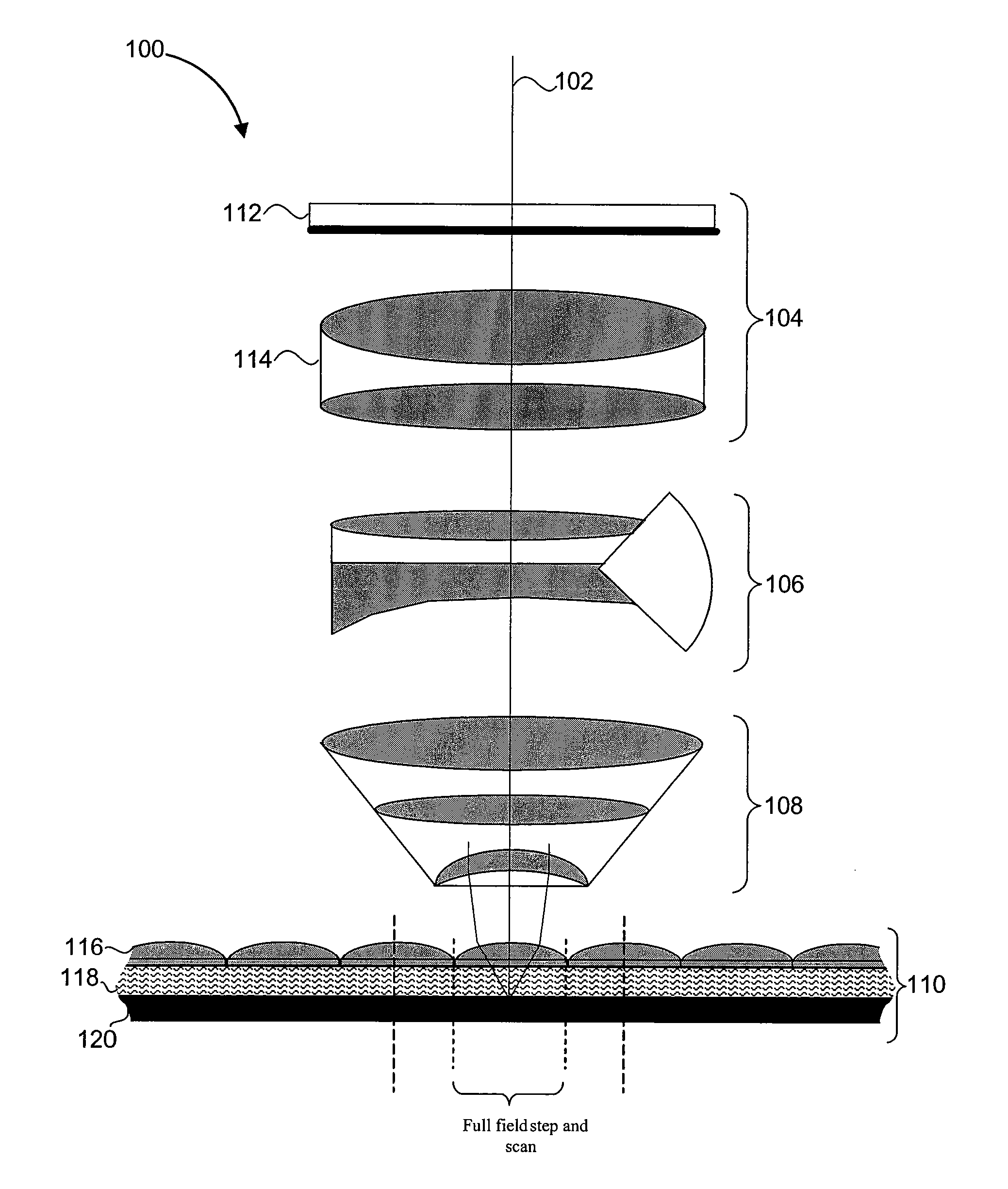
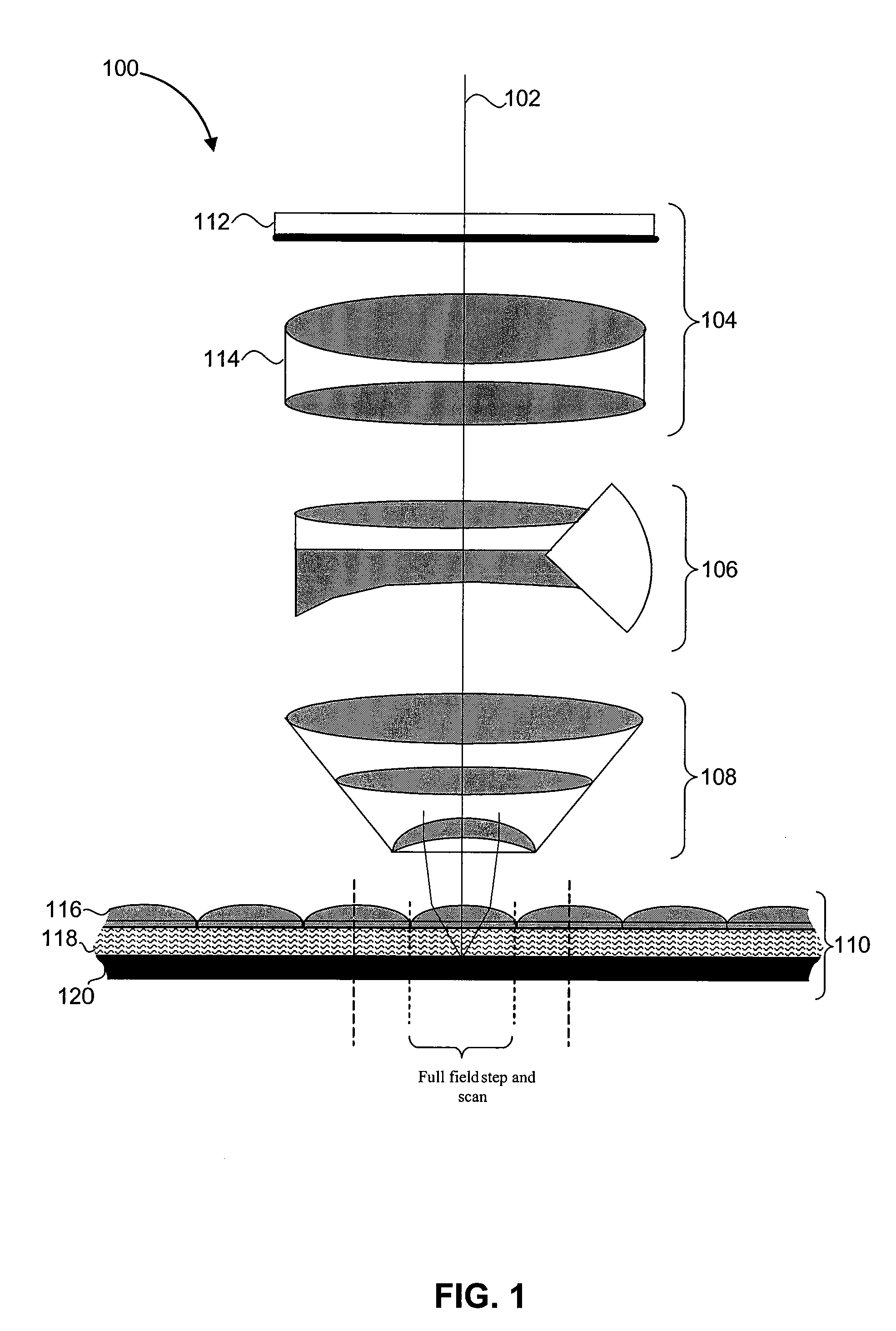
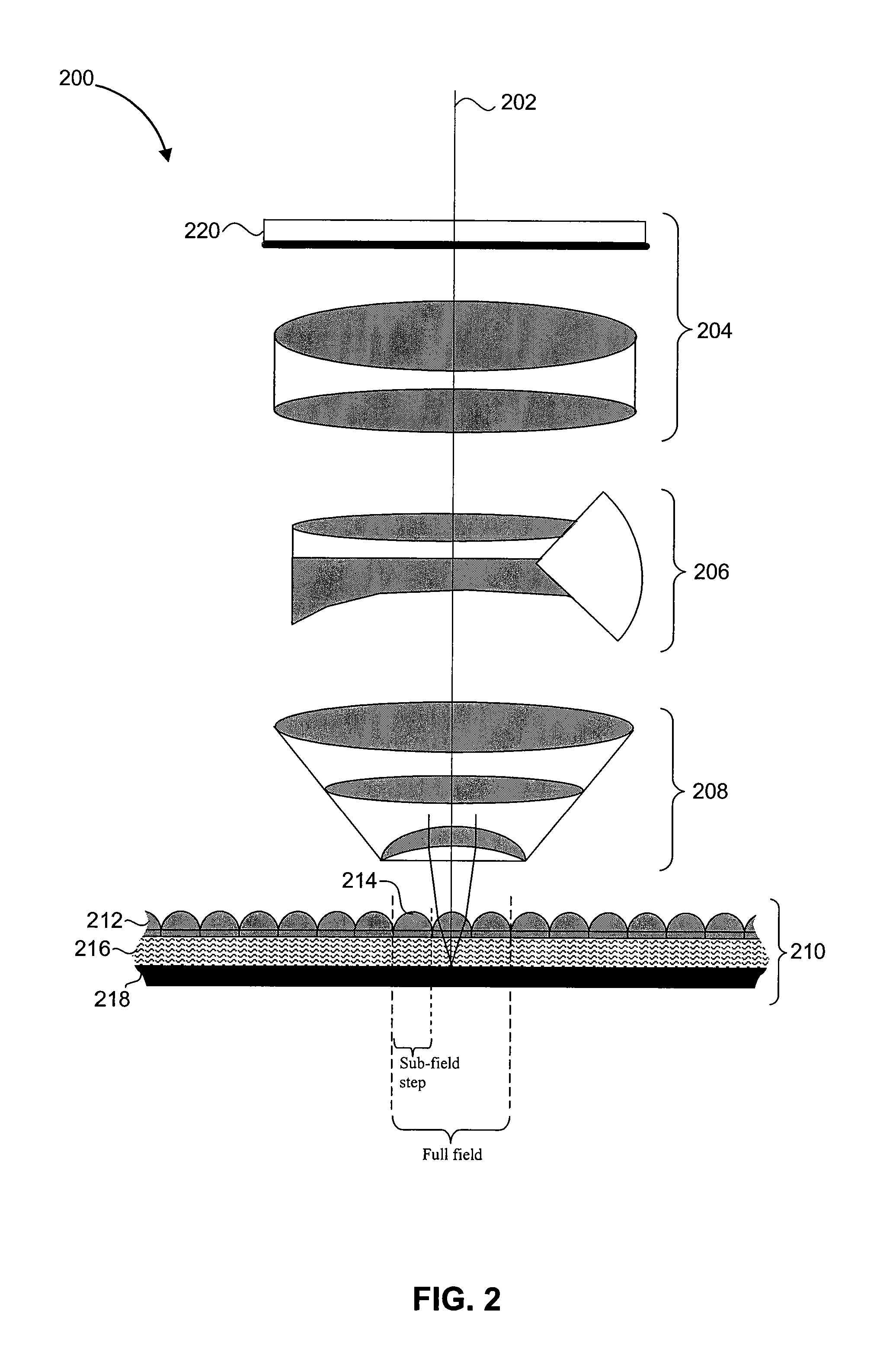
[0041]FIG. 2 is a block diagram of an exposure system 200 according to the present invention. Elements in pattern generator group 204, dynamic axial compensation group 206, and optical group 208 respectively correspond to pattern generator group 104, dynamic axial compensation group 106, and optical group 108 in system 100. Similarly, moveable substrate unit 210 includes an optical power lens array 212, immersion liquid 216, and a substrate 218. Moveable substrate unit 210 can alternatively be inverted (shown in FIG. 6B) in an inverted wafer system, similar to that described above for moveable substrate unit 110.
[0042] Instead of being a step and scan system, system 200 is a step system. Thus, instead of scanning line-by-line through an entire field before stepping, system 200 breaks each field into sub-fields. System 200 steps to each sub-field, and exposes the entire sub-field without scanning. Pattern generator 220 may also need to be moved, since the full field is not imaged in ...
third embodiment
[0044]FIG. 3 is a block diagram of an exposure system 300 according to the present invention. System 300 is a full field step and scan system. Elements in pattern generator group 304, axial displacement compensation group 306, and optical group 308 respectively correspond to pattern generator 104, dynamic axial compensation group 106, and optical group 108 in system 100. Instead of including a lens array in contact with immersion liquid 318, substrate unit 310 includes a flat plate 316 having no optical power. Any optical power that a lens array would have added can instead be included in, for example, optical group 308. Moveable substrate unit 310 can alternatively be inverted (shown in FIG. 6C) in an inverted wafer system, similar to that described above for moveable substrate unit 110.
[0045] Using flat plate 316 instead of a lens array makes this embodiment easy to add to pre-existing systems. All the optics necessary for exposure may be incorporated into optical groups 314 and 3...
PUM
| Property | Measurement | Unit |
|---|---|---|
| wavelengths | aaaaa | aaaaa |
| wavelengths | aaaaa | aaaaa |
| wavelengths | aaaaa | aaaaa |
Abstract
Description
Claims
Application Information


