
Methods of Forming Field Effect Transistors and Capacitor-Free Dynamic Random Access Memory Cells

Inactive Publication Date: 2007-07-19
SAMSUNG ELECTRONICS CO LTD
View PDF9 Cites 33 Cited by
  • Summary
  • Abstract
  • Description
  • Claims
  • Application Information

AI Technical Summary

Benefits of technology

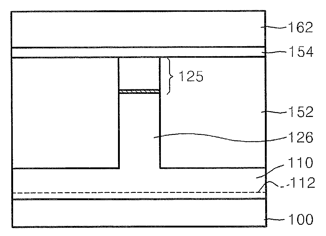
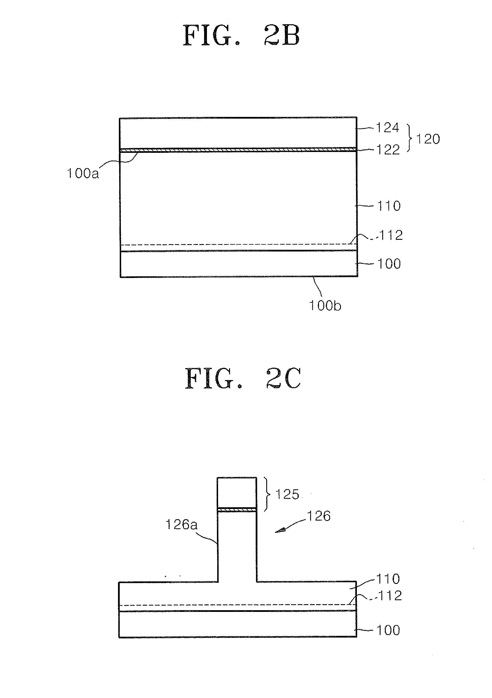
[0011]The front side of the semiconductor wafer is selectively etched to define a channel region protrusion extending therefrom. This etching step is performed using the first electrically insulating layer pattern as an etching mask. A second electrically insulating layer is deposited on sidewalls of the channel region protrusion. This second electrically insulating layer is planarized to define an electrical isolation region surrounding the channel region protrusion. A second semiconductor wafer is then bonded on a planarized surface of the electrical isolation region. Thereafter, a portion of the backside of the first semicond

Problems solved by technology

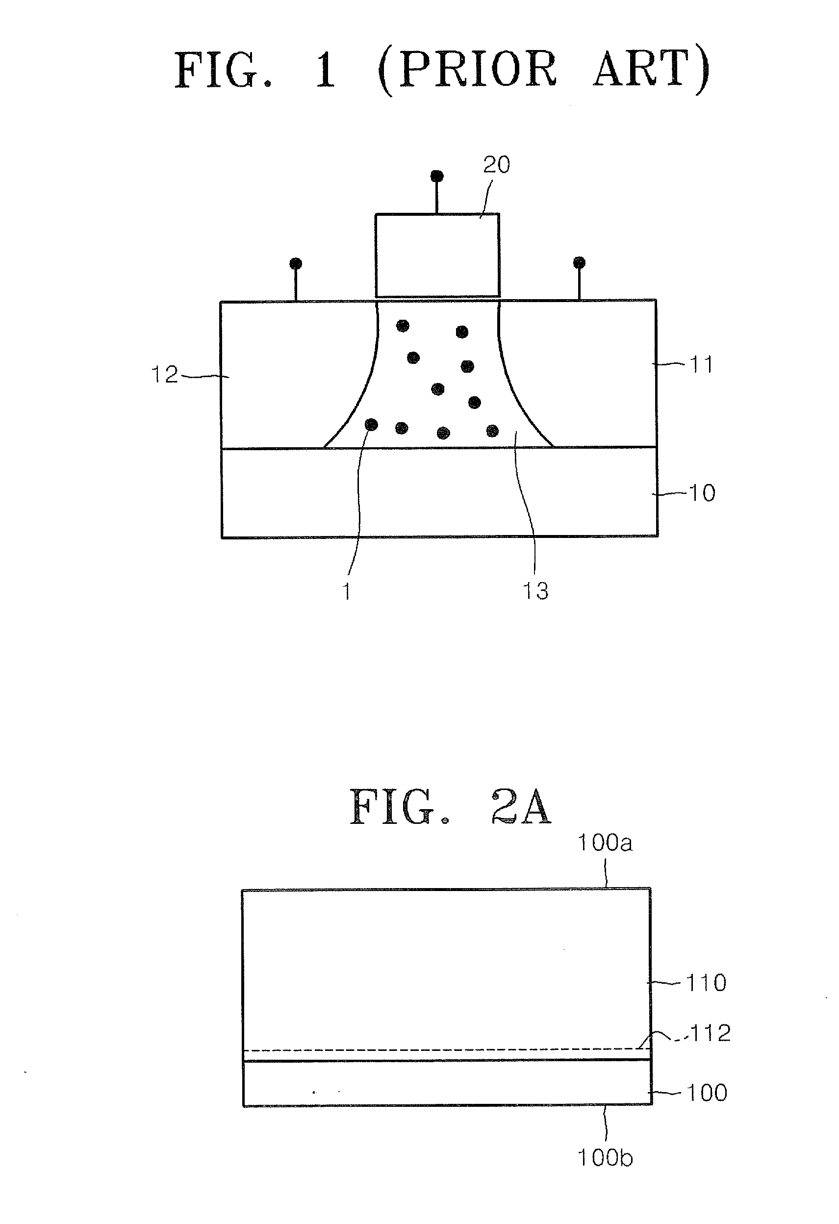
This requirement of periodic refreshing can limit the operation of a capacitor-free DRAM device, particularly if the rate at which refresh operations must be performed to reliably store data becomes excessive.

Method used


Image

  • Methods of Forming Field Effect Transistors and Capacitor-Free Dynamic Random Access Memory Cells
  • Methods of Forming Field Effect Transistors and Capacitor-Free Dynamic Random Access Memory Cells
  • Methods of Forming Field Effect Transistors and Capacitor-Free Dynamic Random Access Memory Cells

Examples


Embodiment Construction

[0014]The present invention will now be described more fully hereinafter with reference to the accompanying drawings, in which preferred embodiments of the invention are shown. This invention may, however, be embodied in different forms and should not be construed as limited to the embodiments set forth herein. Rather, these embodiments are provided so that this disclosure will be thorough and complete, and will fully convey the scope of the invention to those skilled in the art. In the drawings, the thickness of layers and regions are exaggerated for clarity. It will also be understood that when a layer is referred to as being “on” another layer or substrate, it can be directly on the other layer or substrate, or intervening layers may also be present. Moreover, the terms “first conductivity type” and “second conductivity type” refer to opposite conductivity types such as N or P-type, however, each embodiment described and illustrated herein includes its complementary embodiment as...


PUM


Abstract

Methods of forming capacitor-free DRAM cells include forming a field effect transistor by forming a first semiconductor wafer having a channel region protrusion extending therefrom and surrounding the channel region protrusion by an electrical isolation region. A portion of a backside of the first semiconductor wafer is then removed to define a semiconductor layer having a primary surface extending opposite the channel region protrusion and the electrical isolation region. A gate electrode is formed on the primary surface. The gate electrode extends opposite the channel region protrusion. The source and drain regions are formed in the semiconductor layer, on opposite sides of the gate electrode.

Description

CROSS-REFERENCE TO RELATED APPLICATION[0001]This application claims priority to Korean Patent Application No. 10-2006-0004439, filed Jan. 16, 2006, the disclosure of which is hereby incorporated herein by reference.FIELD OF THE INVENTION[0002]The present invention relates to integrated circuit fabrication methods and, more particularly, to methods of forming field effect transistors.BACKGROUND OF THE INVENTION[0003]Conventional dynamic random access memory (DRAM) cells typically utilize a single capacitor (1C) to retain charge representing a “1” or “0” data value and one transistor (1T) having a current carrying terminal (e.g., source terminal) connected to an electrode of the capacitor and a gate terminal connected to a word line. This transistor is frequently referred to as a memory cell access transistor.[0004]More recently, DRAM fabrication techniques have been proposed to reduce a complexity of fabricating conventional 1T / 1C DRAM devices. These techniques include methods of for...

Claims


Application Information

Patent Timeline
IPC IPC(8): H01L21/336
CPCH01L27/108H01L29/7841H01L29/66772H01L27/10802H10B12/20H10B12/00G02F1/1333G06F3/041
Inventor SONG, KI-WHANKIM, CHANG-KYUN
Owner SAMSUNG ELECTRONICS CO LTD
Learn More