Infrared detector elements and methods of forming same

a technology of infrared detector elements and detector elements, which is applied in the direction of material analysis, optical radiation measurement, instruments, etc., can solve the problems of high stress on lid wafers composed of such non-silicon-based visible spectrum-transmissive materials, high cost, and high cost, and achieves fast response, reduces the thermal mass or heat capacity of patterned drc membrane structures, and reduces the thermal response time of suspended membrane structures

Active Publication Date: 2007-07-26
DRS NETWORK & IMAGING SYST
View PDF98 Cites 91 Cited by
  • Summary
  • Abstract
  • Description
  • Claims
  • Application Information

AI Technical Summary

Benefits of technology

[0018]In those embodiments employing a DRC pixel, the thermal mass or heat capacity of the patterned DRC membrane structure is reduced relative to an unpatterned membrane structure, which has the effect or reducing the thermal response time of the suspended membrane structure. This characteristic may be implemented in one embodiment to enable high performing infrared bolometer elements with very short (e.g., less than about 5 milliseconds) time constant. Fast response pixels allow for higher frame rate operation of the infrared FPA (e.g., up to about 120 Hz). In addition, fast response time makes feasible the use of a periodic chopper together with a fast responding bolometer detector element.

Problems solved by technology

However, use of two separate focal plane arrays requires additional space and complicates the structure and circuitry of the imaging assembly.
However, those MEMS devices that require optical transmission in the visible spectrum utilize non-silicon-based window materials (i.e., materials that are primarily composed of a material other than silicon) that are optically transmissive for the visible spectrum.
), lid wafers composed of such non-silicon-based visible spectrum-transmissive materials would be under high stress and fracture during bonding which would not be the case for silicon materials.
However, such a configuration, results in an inherently costly package.

Method used


Image

  • Infrared detector elements and methods of forming same
  • Infrared detector elements and methods of forming same
  • Infrared detector elements and methods of forming same

Examples


Embodiment Construction

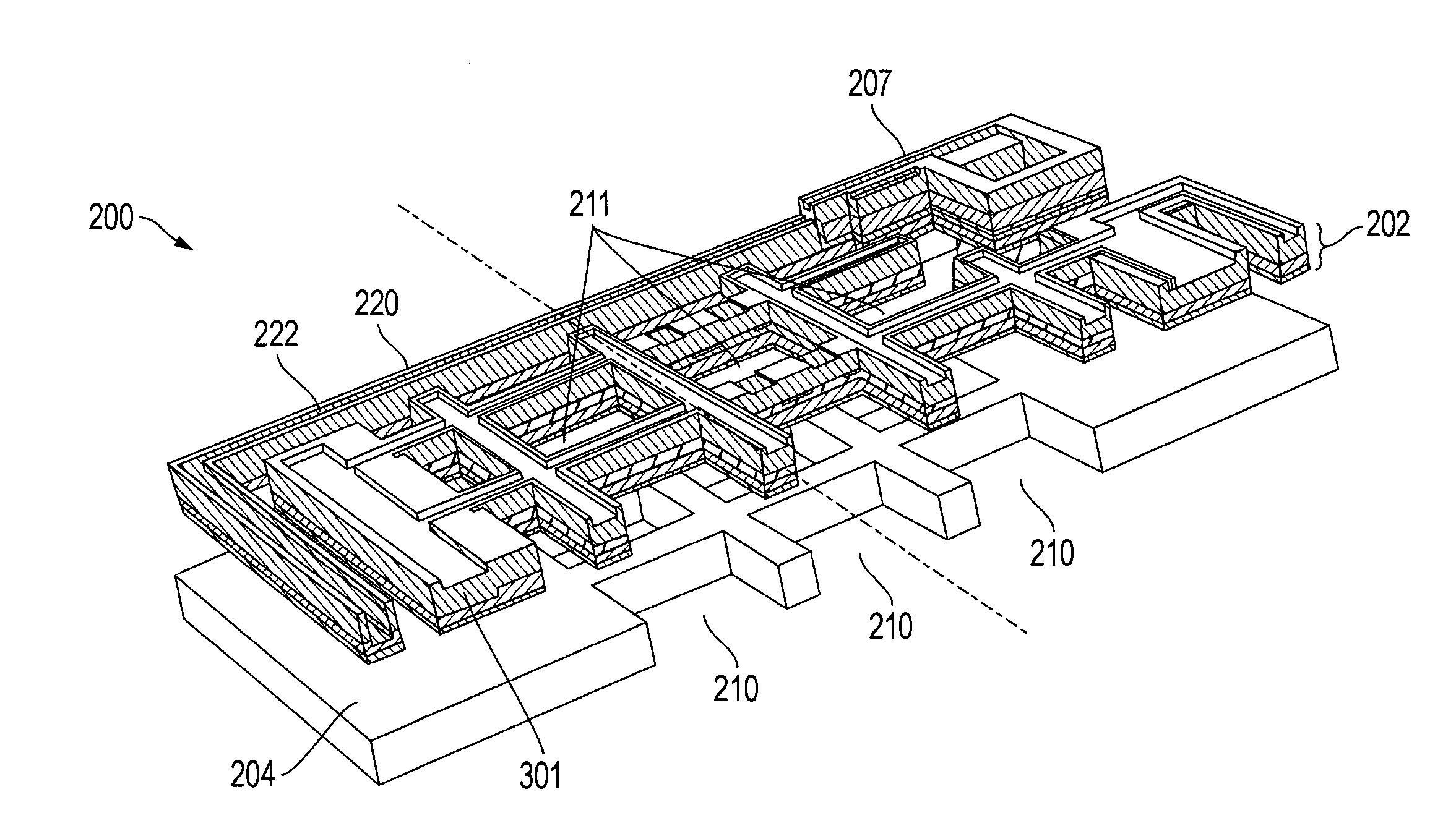
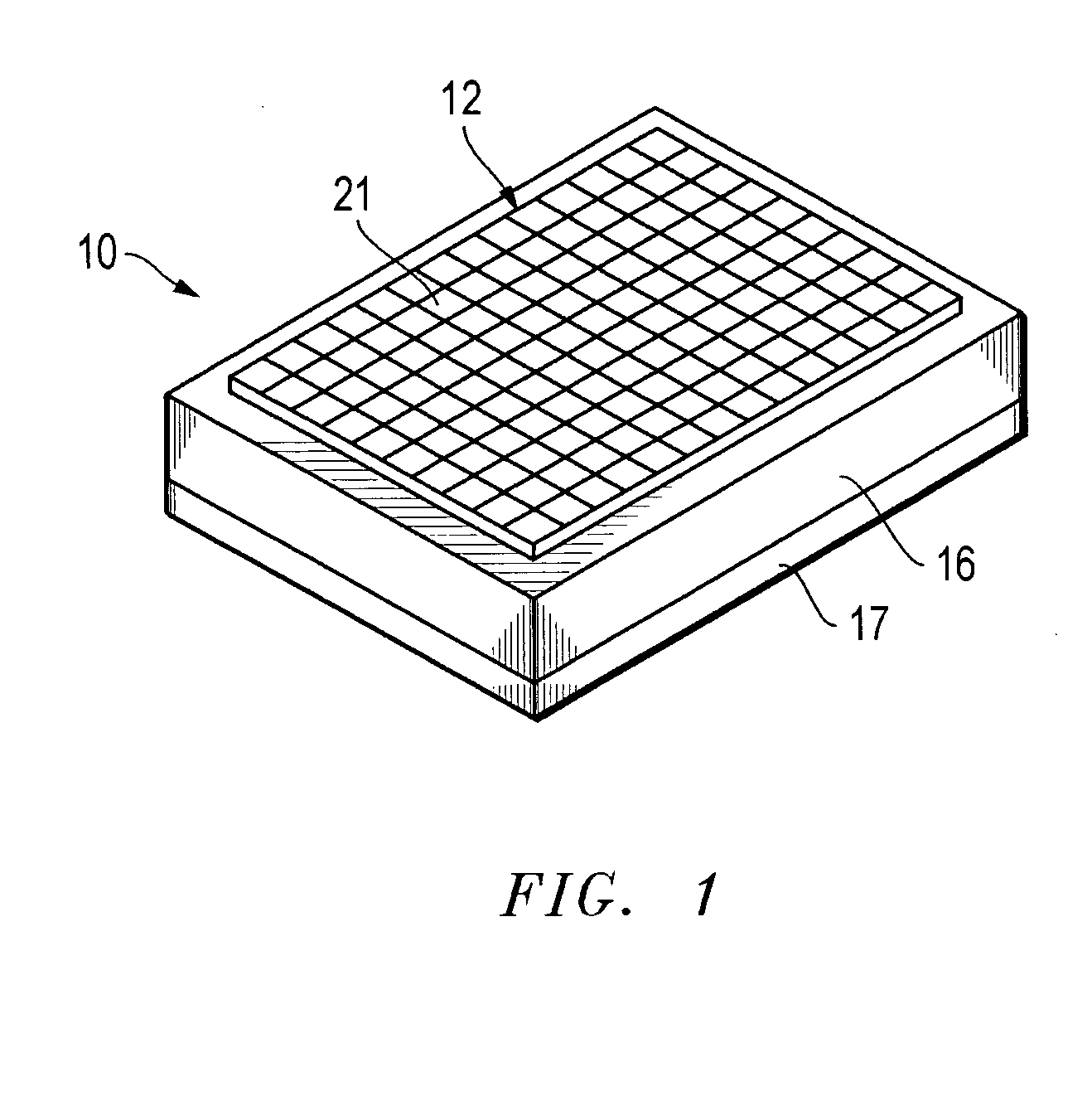
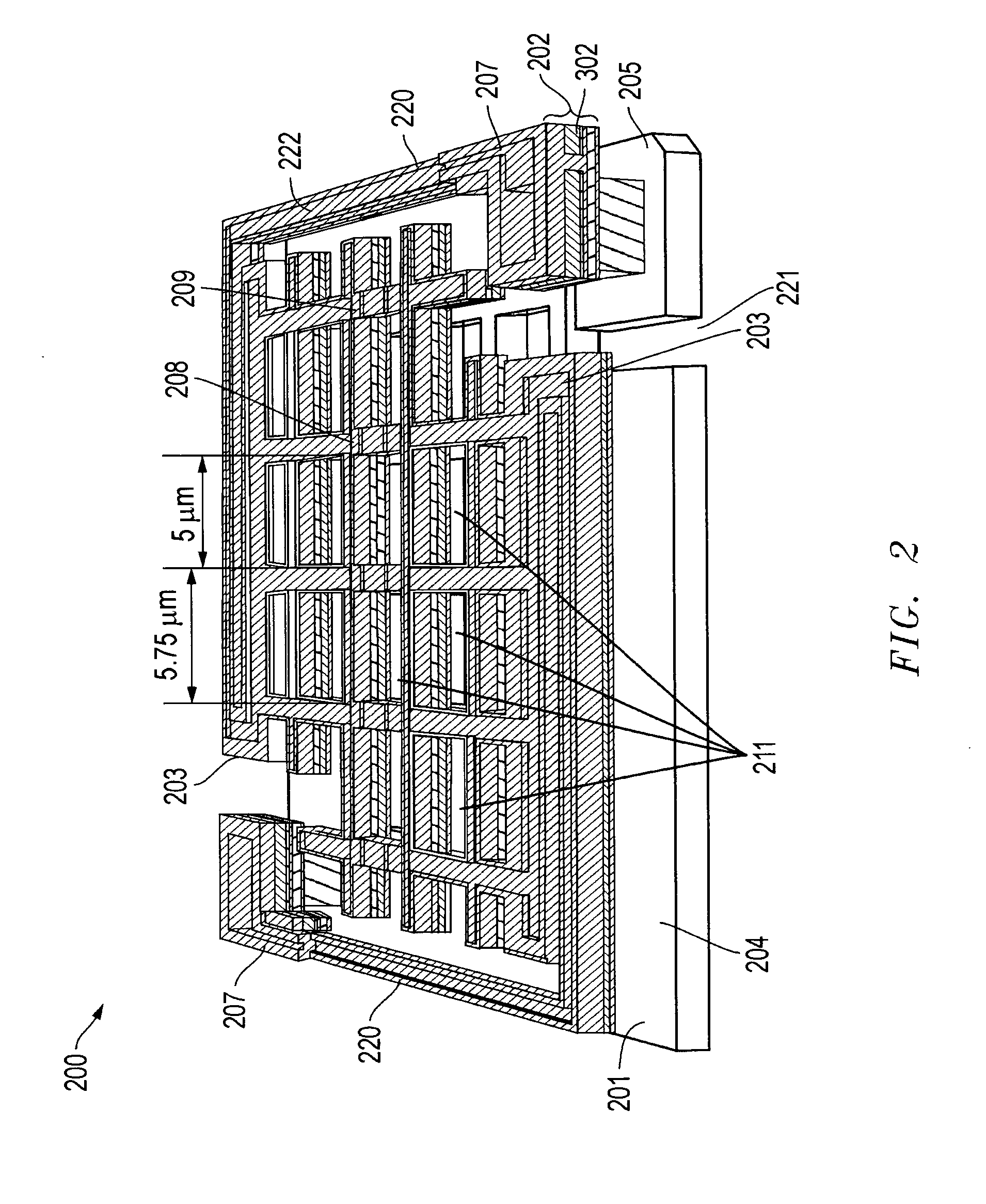
[0055]FIG. 1 is a diagrammatic perspective view of an multi-band detector 10 which may be configured as a dual-band detector according to one embodiment of the disclosed systems and methods to sense visible light and thermal energy and output electrical signals representative of a two-dimensional image of that sensed visible light and / or thermal energy. In this embodiment, the multi-band detector 10 includes a multi-band focal plane array (FPA) 12 disposed on a substrate 16. The substrate 16 includes a ROIC. As will be described further herein, the ROIC may be configured to detect signals representative of visible radiation from each detector element 21 in the focal plane array 12, to integrate the thermally induced electrical signals from each detector element 21 in the focal plane array 12, and to multiplex the signals off the array with the appropriate signal conditioning and processing, e.g., as shown in FIG. 5 with signals provided to column multiplexer (column MUX) via input p...


PUM


Abstract

Infrared detector elements and methods for forming infrared detector elements in which the top metal layer of CMOS circuitry of the detector element is employed as a lead metal reflector for the infrared detector.

Description

[0001]This patent application claims priority to copending U.S. Provisional patent application Ser. No. 60 / 762,252, filed Jan. 26, 2006, and entitled “SYSTEMS AND METHODS FOR INTEGRATING FOCAL PLANE ARRAYS” by Syllaios et al., the entire disclosure of which is incorporated herein by reference.FIELD OF THE INVENTION[0002]This invention relates generally to infrared detector elements, and more particularly to microbolometer infrared detector elements.BACKGROUND OF THE INVENTION[0003]Infrared (IR) detectors are often utilized to detect fires, overheating machinery, planes, vehicles, people, and any other objects that emit thermal radiation. Infrared detectors are unaffected by ambient light conditions or particulate matter in the air such as smoke or fog. Thus, infrared detectors have potential use in night vision and when poor vision conditions exist, such as when normal vision is obscured by smoke or fog. IR detectors are also used in non-imaging applications such as radiometers, gas...

Claims


Application Information

Patent Timeline
Patent Type & Authority Applications(United States)
IPC IPC(8): G01J5/02
CPCG01J5/02G01J5/023G01J5/024G01J5/08G01J2005/0077G01J5/20G01J5/22G01J5/522G01J5/0834G01J5/0804G01J5/53
Inventor SCHIMERT, THOMAS R.SYLLAIOS, ATHANASIOS J.MCCARDEL, WILLIAM L.GOOCH, ROLAND W.
Owner DRS NETWORK & IMAGING SYST
Why Eureka
Try Eureka