Semiconductor device, electronic apparatus comprising the same, and method for fabrication of substrate for semiconductor device used therein

a semiconductor device and electronic apparatus technology, applied in the manufacture of printed circuits, printed circuit aspects, basic electric elements, etc., can solve the problems of affecting the high-frequency characteristics of the electrode terminal position and configuration, affecting the mounting of the circuit component, and affecting the high-frequency characteristics. , to achieve the effect of excellent high-frequency characteristics and excellent high-frequency characteristics

Inactive Publication Date: 2007-07-26
PANASONIC CORP
View PDF4 Cites 8 Cited by
  • Summary
  • Abstract
  • Description
  • Claims
  • Application Information

AI Technical Summary

Benefits of technology

[0019]An object of the present invention is to solve the conventional problems shown above and thereby provide a semiconductor device having high reliability and also having high-frequency characteristics which are not degraded by a mounting process such solder connection and an electronic apparatus comprising a mounting circuit board on which the semiconductor device is mounted.
[0032]The arrangement allows the provision of solder connection between the semiconductor device and the mounting circuit board with excellent high-frequency characteristics and further allows the provision of an electronic apparatus showing excellent high-frequency characteristics by packaging the mounting circuit board in the electronic apparatus.

Problems solved by technology

However, with regard to the mounting of a circuit component such as a chip component, each of the prior patent documents shows only an improvement made to the mounting circuit board on which the circuit component is mounted.
In addition, the mounting of the circuit component is limited to the case where the number of electrode terminals is only two or several.
None of the prior patent documents discloses a structure which typically has the 2-digit number of electrode terminals and a semiconductor bare chip mounted thereon, such as a semiconductor device.
Moreover, in the case where the semiconductor device processes a high-frequency signal, the positions and configurations of the electrode terminals exert delicate and subtle effects on the high-frequency characteristics thereof.
Therefore, without any modification, the approaches disclosed in the prior patent documents cannot be applied directly to the improvement of the electrode structure of the package of the semiconductor device.
As a result, the problem of the significant degradation of the reliability of the semiconductor device 10 occurs.

Method used


Image

  • Semiconductor device, electronic apparatus comprising the same, and method for fabrication of substrate for semiconductor device used therein
  • Semiconductor device, electronic apparatus comprising the same, and method for fabrication of substrate for semiconductor device used therein
  • Semiconductor device, electronic apparatus comprising the same, and method for fabrication of substrate for semiconductor device used therein

Examples


embodiment 1

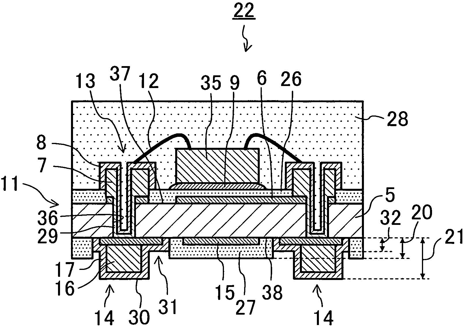
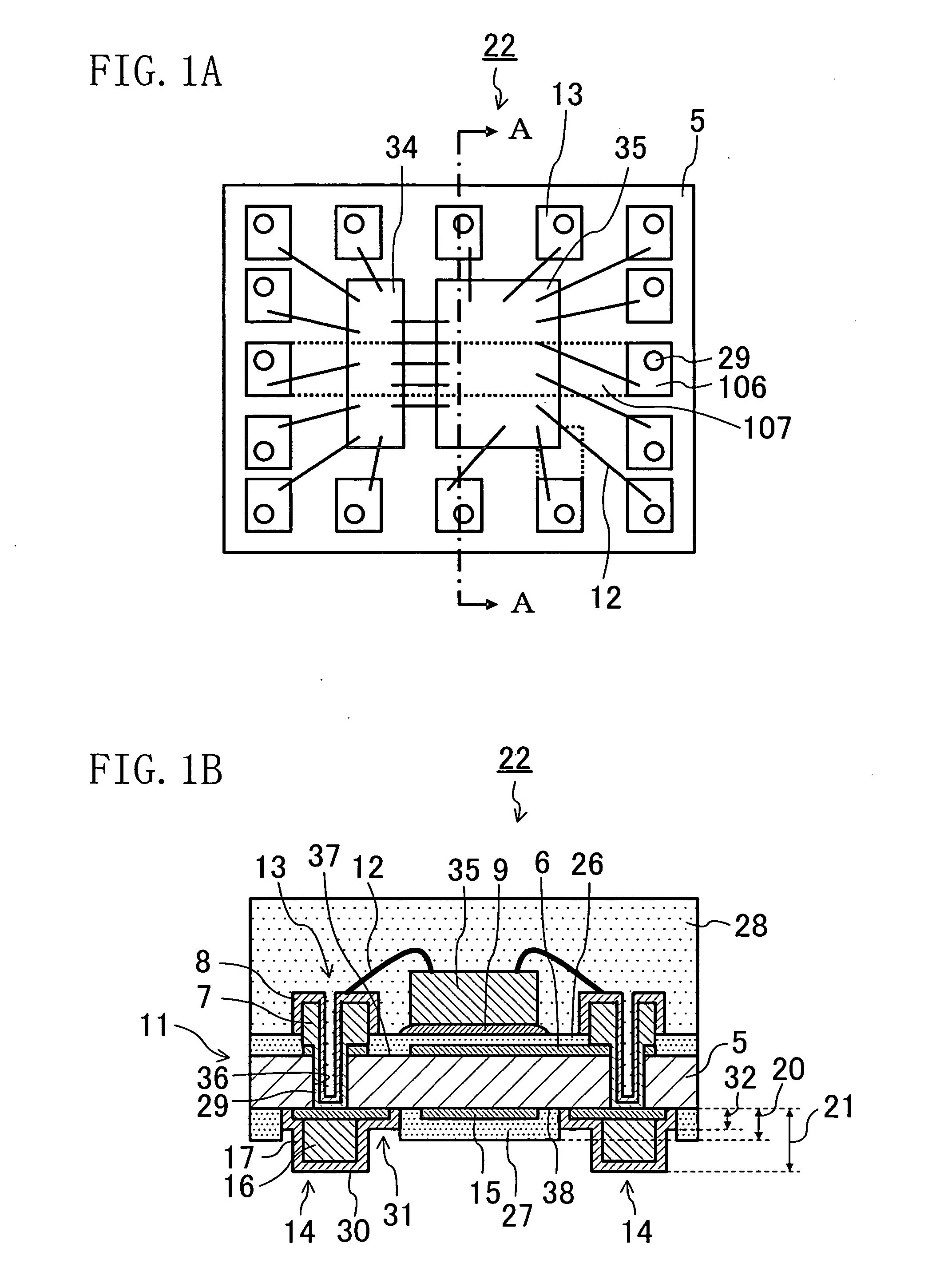
[0042]FIGS. 1A and 1B are views each showing the first embodiment of the present invention. FIG. 1A is a schematic structural view showing a surface on which semiconductor elements are mounted in a semiconductor device 22 according to the present embodiment. FIG. 1B is a cross-sectional view taken along the line A-A of FIG. 1A. FIG. 1A shows a state in which a mold resin portion 28 corresponding to a package upper portion has been removed for easy recognition of the positions of upper electrodes and the semiconductor elements.

[0043]In FIG. 1A, the semiconductor device 22 according to the present embodiment has a structure in which two semiconductor elements 34 and 35 are mounted on a first insulating film 26 on a substrate 5 for semiconductor device as a part of a package. In the vicinity of the four edges of the substrate 5 for semiconductor device, upper electrodes 13 are arranged along the individual edges and connected by conductive wires 12 to the semiconductor elements 34 and ...

embodiment 2

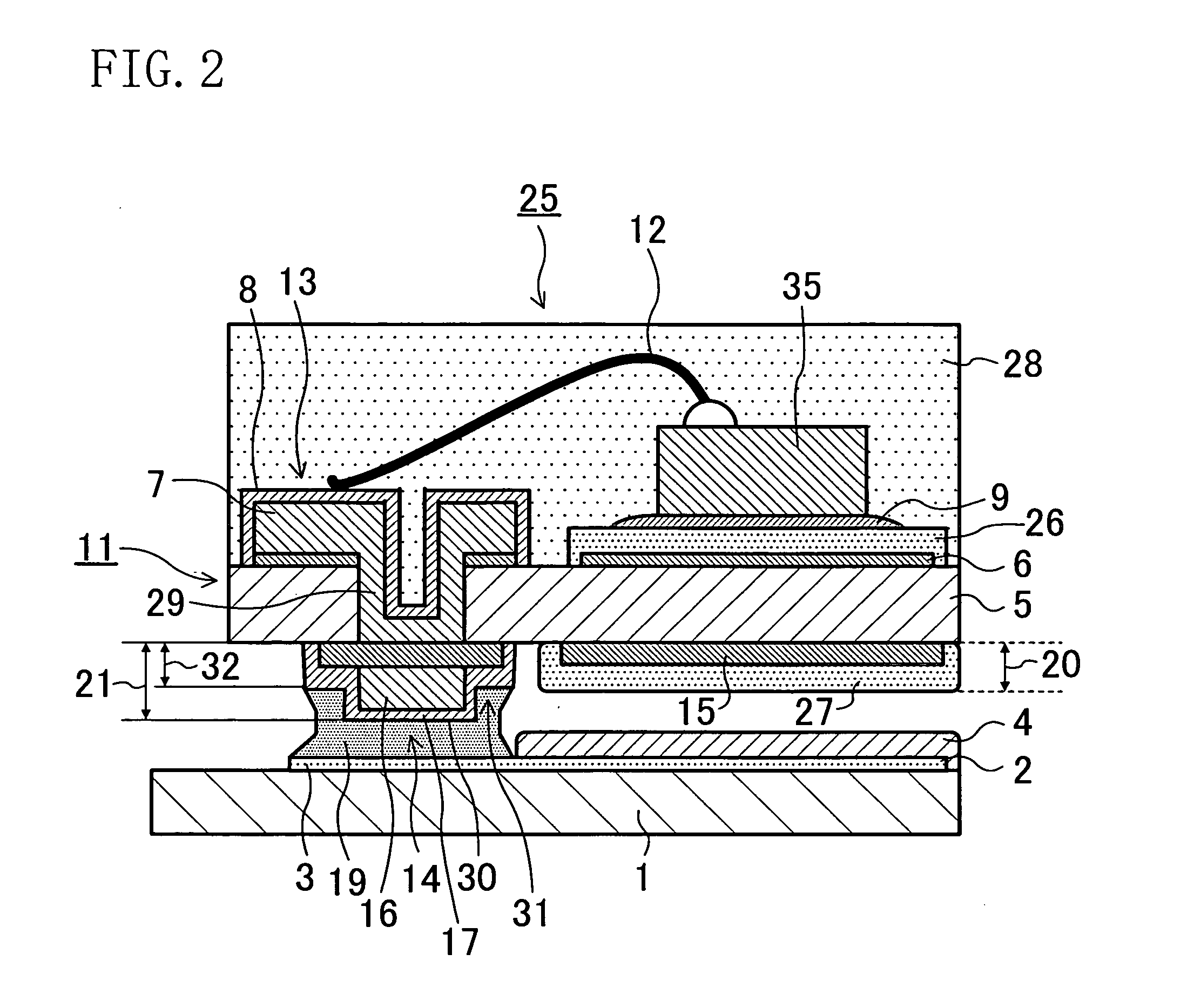
[0062]FIG. 6 is a view showing the second embodiment of the present invention. The second embodiment is different from the first embodiment of FIGS. 1A, 1B, and 2 in the configuration of the external terminal 14. Specifically, each of the external terminals 14 is configured such that the metal plate layer 16 has a stepped portion. The stepped configuration can be implemented by repeating the step of metal plating twice or by forming a thick metal plate layer and then removing a part thereof by etching or the like. As a result, when the second surface 38 of the substrate 5 for semiconductor device is used as a reference height, the height 20 of the second insulating film 27 is positioned between the height 21 to the surface 30 of the external terminal 14 and the height 32 of the stepped portion 31. A detailed description will be given herein below to the portions of the second embodiment which are different than in the first embodiment.

[0063]The external terminal 14 shown in FIG. 6 i...


PUM


Abstract

A semiconductor device has upper electrodes and external terminals which are protruding above the both surfaces of a substrate for semiconductor device and connected to each other by penetrating electrodes, a first insulating film covering at least a metal pattern except for the portions of the first insulating film corresponding to the upper electrodes, a second insulating film covering at least another metal pattern except for the portions of the second insulating film corresponding to the external terminals, and a semiconductor element connected to the upper electrodes and placed on the substrate for semiconductor device. The solder-connected surface of the external terminal is positioned to have a height larger than that of a surface of the second insulating film. The semiconductor element is placed on the first insulating film and covered, together with the upper electrodes, with a mold resin.

Description

CROSS REFERENCE TO RELATED APPLICATIONS[0001]The teachings of Japanese Patent Application JP 2006-18003, filed Jan. 26, 2006, are entirely incorporated herein by reference, inclusive of the specification, drawings, and claims.BACKGROUND OF THE INVENTION[0002]The present invention relates to a semiconductor device on which a high-frequency circuit is mounted and to an electronic apparatus comprising a high-frequency mounting circuit board to which the semiconductor device is connected by soldering.[0003]In recent years, higher-speed operation and increasing miniaturization have been required of electronic apparatuses in an information communication field and in an information processing field. As a representative of these apparatuses, a mobile telephone apparatus can be listed. To increase the operating speed of an apparatus comprising a high-frequency mounting circuit board, such as a mobile telephone apparatus, and reduce the size thereof, it is not only necessary to increase the o...

Claims


Application Information

Patent Timeline
Patent Type & Authority Applications(United States)
IPC IPC(8): H01L23/12
CPCH01L21/4846H01L23/49811H01L2924/12041H01L2224/45144H01L24/49H01L24/48H05K2201/09509H05K2201/0394H05K2201/0367H05K3/3436H05K1/113H01L2924/15311H01L2924/1423H01L2924/01079H01L2924/01078H01L2924/01046H01L2924/01029H01L2924/01013H01L2224/73265H01L2224/49175H01L2224/49171H01L2224/48227H01L2224/48091H01L2224/32225H01L23/49827H01L2924/00014H01L2924/00H01L2924/00012H01L24/45H01L24/73H01L2924/181H01L2224/48465H01L2224/05599
Inventor YOSHIKAWA, NORIYUKITAKEUCHI, NOBORUITOU, KENICHIFUKUDA, TOSHIYUKI
Owner PANASONIC CORP
Why Eureka
Try Eureka