Touch panel, electro-optic device, manufacturing method for electro-optic device and electronic device

a manufacturing method and electrooptic technology, applied in the direction of electric digital data processing, instruments, computing, etc., can solve the problems of touch panel erroneously detecting locations, surface acoustic waves also attenuated, poor impact resistan

Inactive Publication Date: 2007-07-26
SEIKO EPSON CORP
View PDF12 Cites 69 Cited by
  • Summary
  • Abstract
  • Description
  • Claims
  • Application Information

AI Technical Summary

Benefits of technology

[0075]As a result, even if an electro-optic panel and a touch panel are formed as a single unit, there is no loss of the light that is emitted from a backlight and this light can be made visible to an observer on the touch panel side.

Problems solved by technology

However, in a typical ultrasonic surface acoustic wave type of touch panel, because surface acoustic waves are generated on the topmost surface, the surface acoustic waves also become attenuated if water droplets or oil droplets, or dirt or the like are adhering to this topmost surface.
Because of this, an ultrasonic surface acoustic wave type of touch panel erroneously detects locations where water or oil droplets or dirt have adhered as positions touched by a user's finger or the like.
In a touch panel device disclosed in Japanese Unexamined Patent Application, First Publication No. 2004-348686, because the touch panel is formed by a single glass substrate, it has poor impact resistance and when the glass has been formed as a particularly thin plate, there is a problem in that it is broken by only a slight impact.
However, in a transparent resin film (glass substrate), because there is a high modulus of elasticity (Young's modulus), the resin film is not sufficiently bent by the pressing of the user and it is not possible to attenuate the surface acoustic waves being transmitted over the glass substrate surface.
As a result, there is a problem in that it has not been possible to detect the precise position pressed by a user and input malfunctions occur.
However, because surface acoustic waves are generally from several MHz to several 10s of MHz and the detected voltage is also extremely small, there are cases when surface acoustic waves change in a position not being pressed due to the effects of electromagnetic noise generated, for example, by other portions of the product.
This becomes noise and generates malfunctioning in the touch panel.

Method used


Image

  • Touch panel, electro-optic device, manufacturing method for electro-optic device and electronic device
  • Touch panel, electro-optic device, manufacturing method for electro-optic device and electronic device
  • Touch panel, electro-optic device, manufacturing method for electro-optic device and electronic device

Examples


first embodiment

[0084]Liquid Crystal Display Device

[0085]Firstly, a liquid crystal display device 100 including a touch panel according to a first embodiment of this invention will be described.

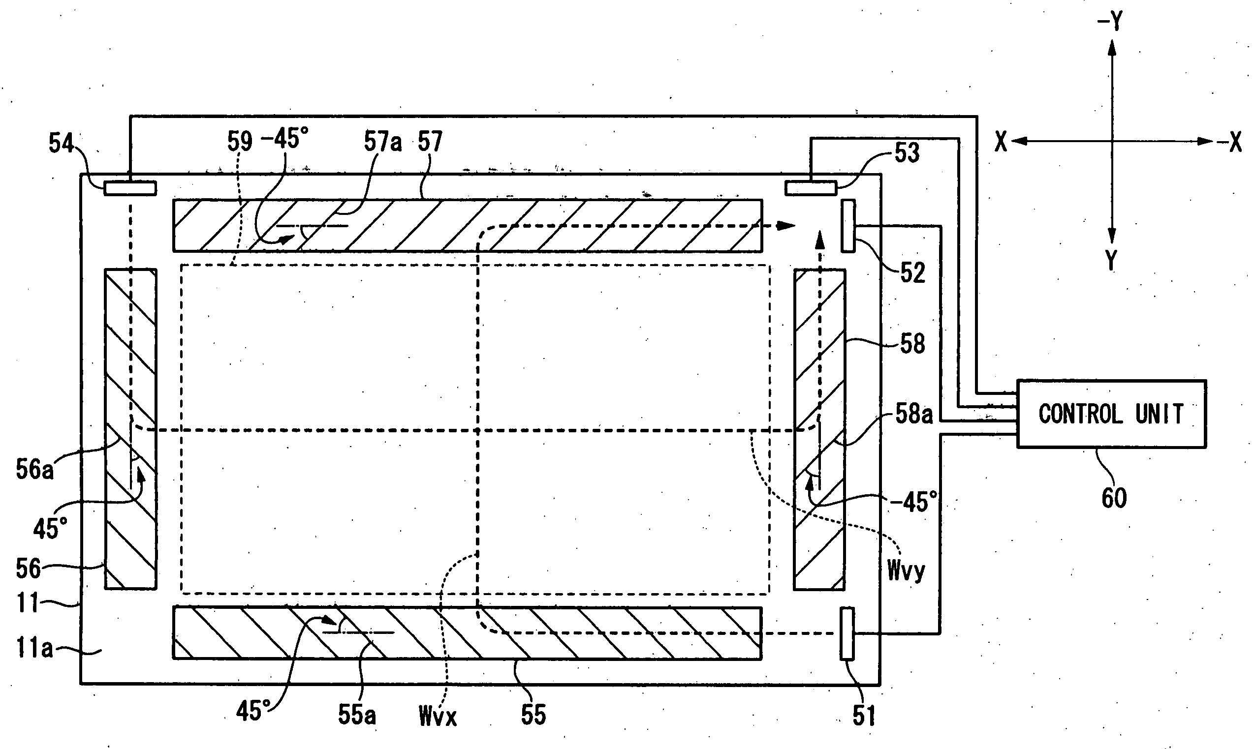
[0086]FIG. 1 is a cross-sectional view showing in typical form a schematic structure of the liquid crystal display device 100 including a touch panel according to the first embodiment.

[0087]In the embodiments described below, this invention is applied to a liquid crystal display device.

[0088]In FIG. 1, the liquid crystal display device 100 (an electro-optic device) is broadly separated into a liquid crystal display panel 30 (an electro-optic panel) and a touch panel 50.

[0089]Firstly, the structure of the liquid crystal display panel will be described with reference made to FIG. 1.

[0090]Surfaces of an element substrate 1 and a color filter substrate 2 that is closer to the liquid crystal layer is called an inner side, while a surface on the opposite side from the liquid crystal layer is called an outer side.

[...

second embodiment

[0224]Next, this embodiment will be described with reference made to the drawings.

[0225]In the above described first embodiment, a touch panel was constructed using a pair of thin substrates.

[0226]In contrast, this second embodiment differs in that a touch panel is constructed using a pair of touch panel substrates, namely, a first touch panel substrate (thin substrate 11) and a second touch panel substrate.

[0227]The rest of the basic structure of the liquid crystal display device is the same as in the first embodiment. Therefore, the same reference numerals are used for common component elements and a detailed structure thereof is omitted.

[0228]FIG. 6 is a cross-sectional view showing the schematic structure of the liquid crystal display device 100 according to this embodiment.

[0229]As shown in FIG. 6, a touch panel 50 has a first touch panel substrate 11 that has been made thinner by etching, and a second touch panel substrate 14 that is arranged so as to face the first touch pane...


PUM


Abstract

A touch panel includes: a first touch panel substrate having a first surface and having a flexibility; a second touch panel substrate arranged a fixed distance away from the first touch panel substrate via spacers, having a second surface that faces the first surface; a position detecting section formed on the first surface, and detecting a position where the first touch panel substrate is being pressed based on changes in surface acoustic waves generated on the first surface; and a resin film formed on the second surface.

Description

CROSS-REFERENCE TO RELATED APPLICATION[0001]This application claims priority from Japanese Patent Application No. 2006-017331, filed Jan. 26, 2006, the contents of which are incorporated herein by reference.BACKGROUND[0002]1. Technical Field[0003]The present invention relates to a touch panel, an electro-optic device, a manufacturing method for an electro-optic device and an electronic device.[0004]2. Related Art[0005]In recent years, in conjunction with the increasing use of small information electronic devices such as personal digital assistants (PDA) and palm top computers, liquid crystal display devices that have a touch panel mounted as an input device on a liquid crystal panel have become widely used.[0006]An example of this type of touch panel is an ultrasonic surface acoustic wave system includes: a glass substrate, a transmitter that transmits a surface acoustic wave over a surface of the glass substrate, and a receiver that detects transmitted surface acoustic waves.[0007]...

Claims


Application Information

Patent Timeline
Patent Type & Authority Applications(United States)
IPC IPC(8): G06F3/043
CPCG06F3/0436G06F3/0412
Inventor SAKURAI, SHINJITAGUCHI, SATOSHIFUNASAKA, TSUKASA
Owner SEIKO EPSON CORP
Why Eureka
Try Eureka