Liquid crystal apparatus and electronic device

a technology of liquid crystal apparatus and electronic device, which is applied in the direction of instruments, non-linear optics, optics, etc., can solve the problems of display quality degradation and transmittance decrease, and achieve the effect of high aperture ratio

Inactive Publication Date: 2007-07-26
EPSON IMAGING DEVICES CORP
View PDF99 Cites 102 Cited by
  • Summary
  • Abstract
  • Description
  • Claims
  • Application Information

AI Technical Summary

Benefits of technology

[0011]An advantage of some aspects of the invention is that it provides an FFS-mode liquid crystal apparatus that can realize a high aperture ratio and also provides an electronic device that includes the liquid crystal apparatus.

Problems solved by technology

Therefore, liquid crystal molecules directly above the pixel electrode are not sufficiently driven, so that transmittance decreases.
This results in degradation in display quality.

Method used


Image

  • Liquid crystal apparatus and electronic device
  • Liquid crystal apparatus and electronic device
  • Liquid crystal apparatus and electronic device

Examples


first embodiment

Structure of Liquid Crystal Apparatus

[0043]The structure of a liquid crystal apparatus 100 according to a first embodiment of the invention is described below with reference to FIG. 1 and other figures.

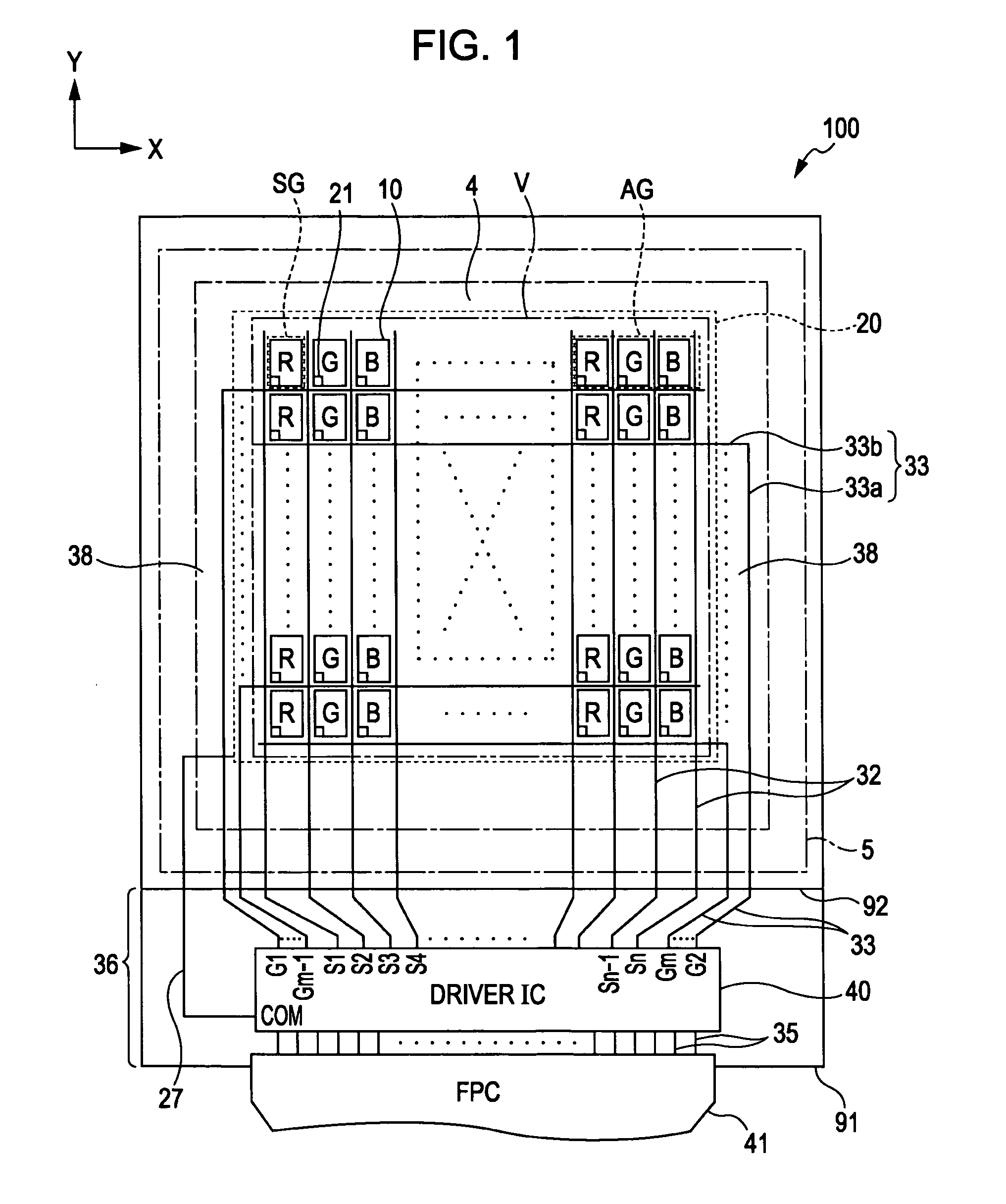
[0044]FIG. 1 is a plan view that shows a schematic structure of the liquid crystal apparatus 100 according to the first embodiment. A color filter substrate 92 is disposed at the front of the drawing (near a viewer), and an element substrate 91 is disposed at the back of the drawing. In FIG. 1, the vertical direction (column) is defined as the y direction, and the horizontal direction (row) is defined as the x direction. In FIG. 1, a region corresponding to each of red, green, and blue (RGB) colors constitutes a single subpixel region SG, and a pixel matrix of subpixel regions SGs of one row and three columns constitutes a single pixel region AG. Hereinafter, one display region existing in one subpixel region SG is sometimes referred to as “subpixel”, and a display region correspondin...

second embodiment

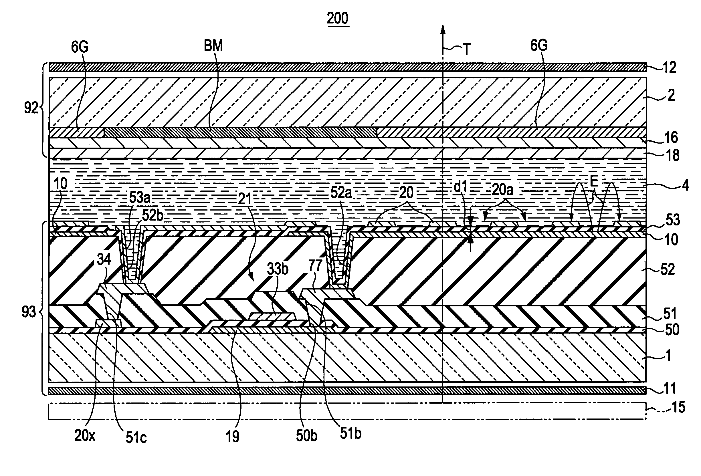
[0092]The structure of a liquid crystal apparatus 200 according to a second embodiment is described below with reference to FIGS. 6 and 7. The liquid crystal apparatus 200 according to the second embodiment is an FFS-mode liquid crystal apparatus including an LTPS-TFT element 21 and is of a transmissive type. In the second embodiment, the same reference numerals are used as in the first embodiment for similar components, and the components are simply described or the description thereof is omitted.

[0093]FIG. 6 shows a two-dimensional structure of four pixels in an element substrate 93 according to the second embodiment. FIG. 7 shows a cross-section view taken along the line VII-VII in FIG. 6 and shows a cross-sectional structure of one subpixel taken from a position through one of the LTPS-TFT elements 21.

[0094]The pixel arrangement in the element substrate 93 according to the second embodiment is first described below with reference to FIGS. 6 and 7.

[0095]A low-temperature polysili...


PUM

PropertyMeasurementUnit
capacitanceaaaaaaaaaa

Abstract

A liquid crystal apparatus includes a substrate that retains liquid crystal, a switching element provided in the substrate, a first insulating film above the switching element, a first electrode above the first insulating film, a second insulating film above the first electrode, and a second electrode above the second insulating film. The second electrode has a plurality of slits and produces an electric field between the first electrode and the second electrode via each of the slits.

Description

BACKGROUND[0001]1. Technical Field[0002]The present invention relates to a liquid crystal apparatus and an electronic device suited for use in displaying various types of information.[0003]2. Related Art[0004]Generally, display modes of liquid crystal apparatus are broadly divided into the twisted nematic (TN) mode, vertical alignment mode, which aims at a wider viewing angle and high contrast, and transverse electric field mode, typified by In-plane switching (IPS) mode and fringe field switching (FFS) mode.[0005]The IPS mode is a mode in which an electric field is applied to liquid crystal substantially in parallel with a substrate. This mode has the advantage of an improved visual characteristic, compared with the TN mode.[0006]However, in an IPS-mode liquid crystal apparatus, a pixel electrode formed from a transparent conductive material, such as indium tin oxide (ITO), and a common electrode for producing a lateral electric field between the common electrode and the pixel elec...

Claims


Application Information

Patent Timeline
Patent Type & Authority Applications(United States)
IPC IPC(8): G02F1/136
CPCG02F1/133512G02F1/134363G02F2001/134372G02F1/136227G02F2001/134318G02F1/136213G02F1/134309G02F1/134372G02F1/1343
Inventor FUJITA, SHINMATSUSHIMA, TOSHIHARU
Owner EPSON IMAGING DEVICES CORP
Why Eureka
Try Eureka