Joining method, method of mounting semiconductor package using the same, and substrate-joining structure prepared by the joining method

a technology of semiconductor package and joining method, which is applied in the direction of soldering apparatus, sustainable manufacturing/processing, final product manufacturing, etc., can solve the problems of affecting the reliability of electronic components sensitive to temperature, difficulty in using temperature-sensitive electronic components, and bending of temperature-sensitive pkg, so as to reduce or prevent the crack caused by coarsened bismuth, the effect of safely mounting

Inactive Publication Date: 2007-07-26
SAMSUNG ELECTRONICS CO LTD
View PDF27 Cites 29 Cited by
  • Summary
  • Abstract
  • Description
  • Claims
  • Application Information

AI Technical Summary

Benefits of technology

[0046] Therefore, by providing a joining method capable of being performed at a lower temperature according to example embodiments of the present invention, junction failure caused due to a bent substrate may be reduced or prevented, and cracks caused due to coarsened bismuth may be reduced or suppressed.
[0047] Further, by employing a joining method according to example embodiments of the present invention,

Problems solved by technology

Because tin (Sn)-silver (Ag) solder has a higher junction temperature, it may be difficult to use for temperature-sensitive electronic components.
In this conventional bonding method, the solder ball and the solder paste are formed of the same composition containing tin, silver and copper, respectively, and reflow at a relatively high temperature of 250° C. through 260° C. As a result, there is a problem in that the temperature-sensitive PKG may be bent.
Such a problem may negatively influence the reliability of electronic components sensitive to temperature.
As illustrated in FIG. 1, because the junction is performed at a relatively high temperatur

Method used


Image

  • Joining method, method of mounting semiconductor package using the same, and substrate-joining structure prepared by the joining method
  • Joining method, method of mounting semiconductor package using the same, and substrate-joining structure prepared by the joining method
  • Joining method, method of mounting semiconductor package using the same, and substrate-joining structure prepared by the joining method

Examples


Embodiment Construction

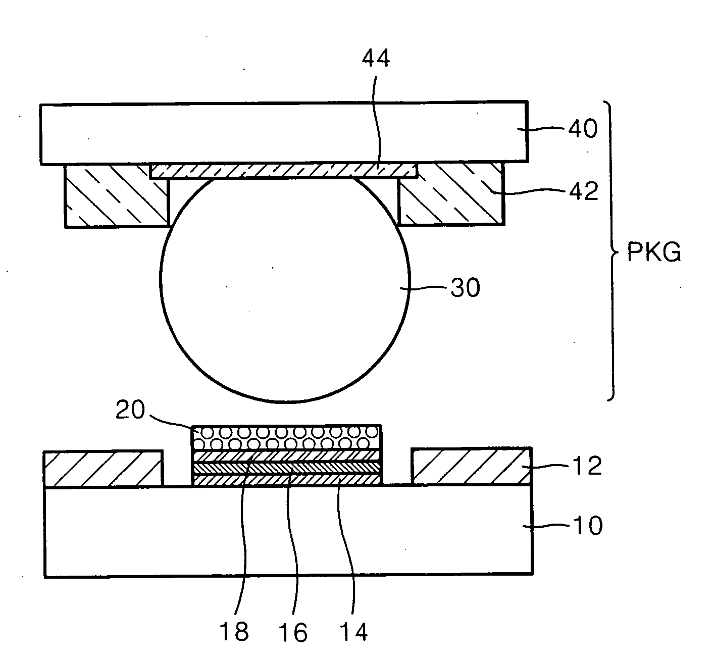
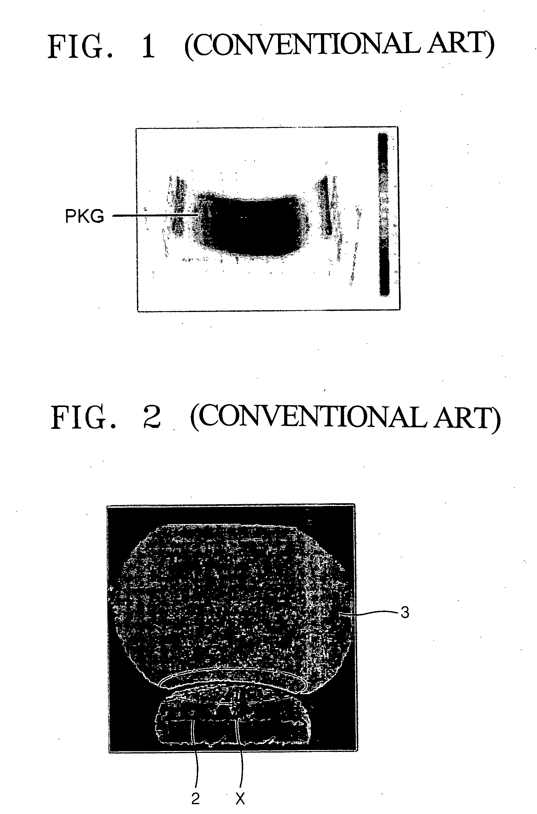
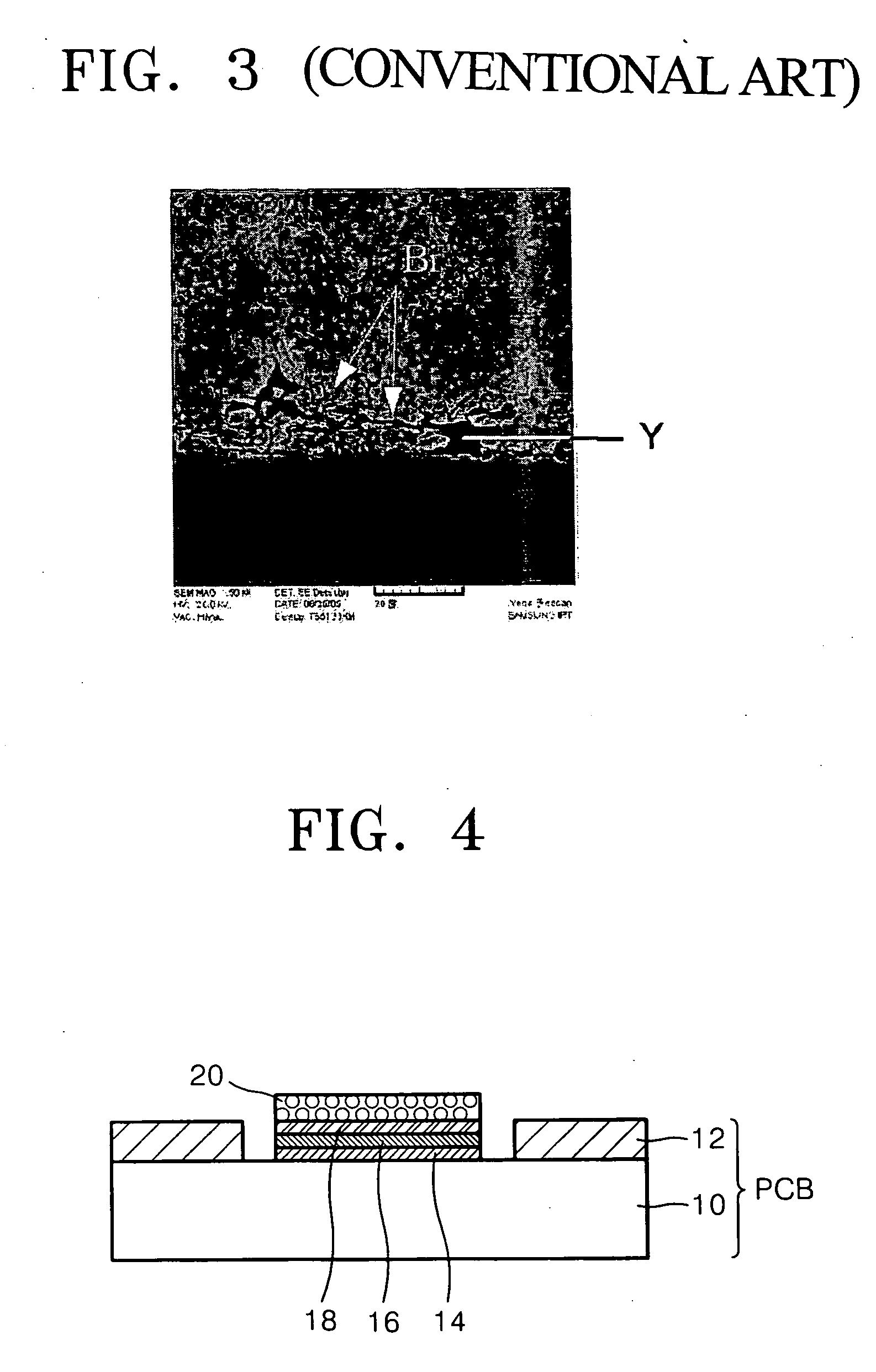
[0056] Various example embodiments of the present invention will now be described more fully with reference to the accompanying drawings in which some example embodiments of the invention are shown. In the drawings, the thicknesses of layers and regions are exaggerated for clarity.

[0057] Detailed illustrative embodiments of the present invention are disclosed herein. However, specific structural and functional details disclosed herein are merely representative for purposes of describing example embodiments of the present invention. This invention may, however, may be embodied in many alternate forms and should not be construed as limited to only the embodiments set forth herein.

[0058] Accordingly, while example embodiments of the invention are capable of various modifications and alternative forms, embodiments thereof are shown by way of example in the drawings and will herein be described in detail. It should be understood, however, that there is no intent to limit example embodi...


PUM

PropertyMeasurementUnit
Temperatureaaaaaaaaaa
Percent by massaaaaaaaaaa

Abstract

A joining method, a method of mounting a semiconductor package (PKG) using the same, and a substrate-joining structure prepared thereby are provided. The joining method may comprise placing a first junction composition including tin and silver, and a second junction composition, including tin and bismuth to contact each other and forming a junction by performing a thermal treatment on the junction compositions at a temperature of at least 170° C. or higher.

Description

PRIORITY STATEMENT [0001] This application claims the benefit of Korean Patent Application No. 10-2006-0007267, filed on Jan. 24, 2006, in the Korean Intellectual Property Office, the disclosure of which is incorporated herein in its entirety by reference.BACKGROUND [0002] 1. Field of the Invention [0003] Example embodiments of the present invention relate to a method of joining a package and the like with a substrate at a low temperature. [0004] 2. Description of the Related Art [0005] To join elements or bodies, conventional bonding methods may apply heat to a metal composition. For example, there are known soldering methods for joining elements or bodies by melting a third material having a melting point lower than that of the elements or bodies to be joined. The third material may be a solder. [0006] Conventionally, an alloy containing lead (Pb) has been used as solder. Because lead has a property of melting (and hence, joining) at a relatively low temperature, lead has been com...

Claims


Application Information

Patent Timeline
IPC IPC(8): B32B15/01
CPCB23K35/0244Y10T428/12708B23K35/262B23K2201/40B32B15/01B32B15/018C22C13/00C22C13/02H05K3/3436H05K3/3463H05K3/3473H05K3/3484H05K2201/10992H01L2224/16225B23K35/025B23K2101/40H01L24/05H01L2224/05023H01L2224/0508H01L2224/05147H01L2224/05155H01L2224/05568H01L2224/05573H01L2224/05644H01L2224/05655H05K3/3485Y02P70/50H01L2924/00014A61F7/007A61H1/008A61H39/04A61H39/06A61H2201/1215A61H2201/1669A61H2203/0456
Inventor KIM, SI-SUKYU, KWANG-SULEE, DONG-CHUNCHOI, JAE-HOON
Owner SAMSUNG ELECTRONICS CO LTD
Why Eureka
Try Eureka