Display device

Inactive Publication Date: 2007-08-02
SEMICON ENERGY LAB CO LTD
View PDF99 Cites 45 Cited by
  • Summary
  • Abstract
  • Description
  • Claims
  • Application Information

AI Technical Summary

Benefits of technology

[0022]With a simple structure in which a plurality of polarizers having different wavelength distributions of extinction coefficients are stacked and provided so that their absorption axes are

Problems solved by technology

Further, there is a problem in that a polarizing plate having a higher degree of polarization is expensive.
A method for improving a contrast ratio by using three polarizing pla

Method used


Image

  • Display device
  • Display device
  • Display device

Examples


embodiment modes

[0060]Hereinafter, embodiment modes and an embodiment of the present invention will be explained with reference to the drawings. Note that it is easily understood by those skilled in the art that forms and details of the invention can be variously changed without departing from the spirit and scope of the invention. Therefore, the present invention should not be construed as being limited to the content of the embodiment modes. Note that common portions and portions having similar functions are denoted by the same reference numerals in all diagrams for describing embodiment modes, and description thereof will not be repeated.

embodiment mode 1

[0061]In this embodiment mode, a concept of a display device in which a pair of stacked layers each including a polarizer using the present invention is provided will be explained.

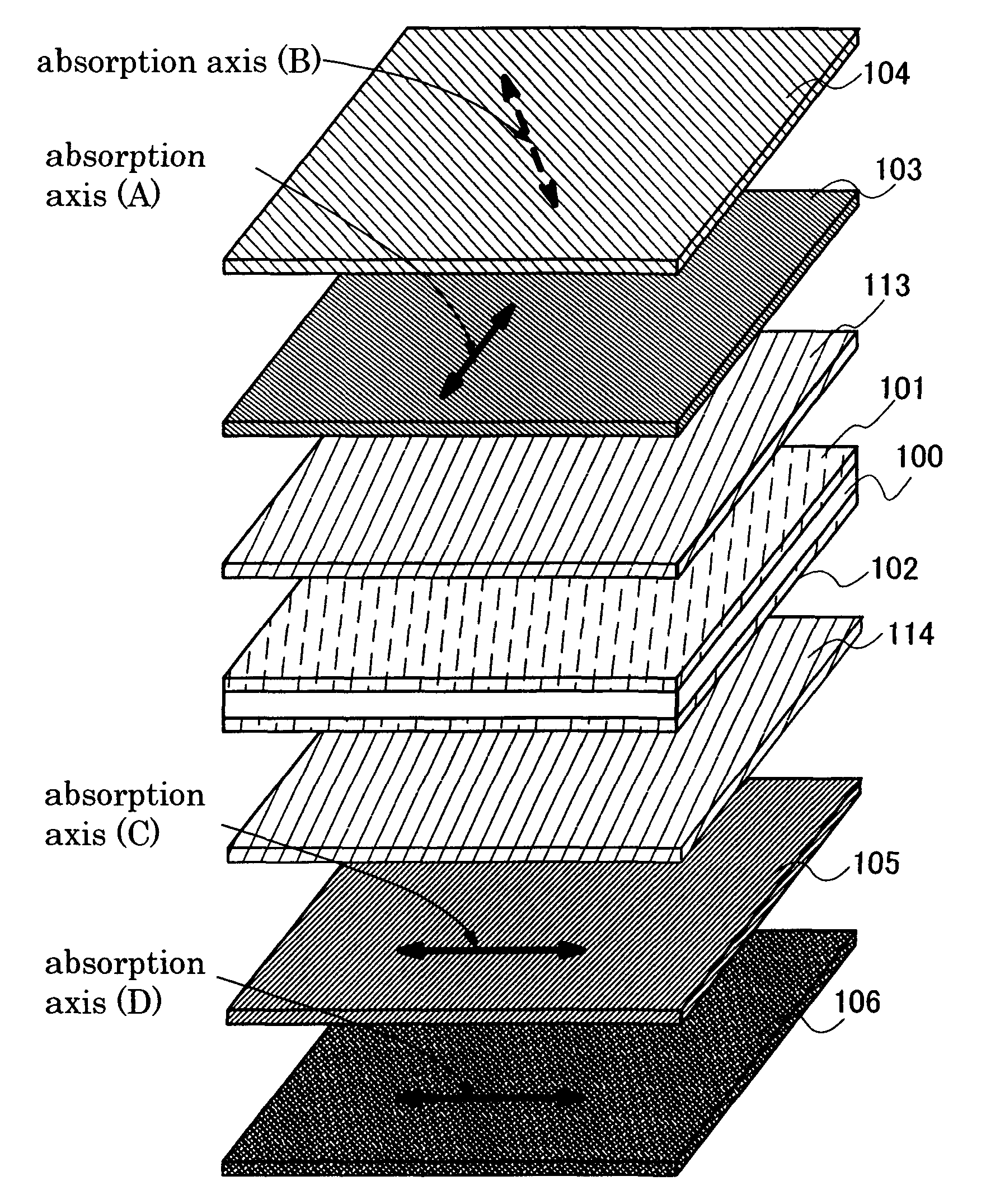
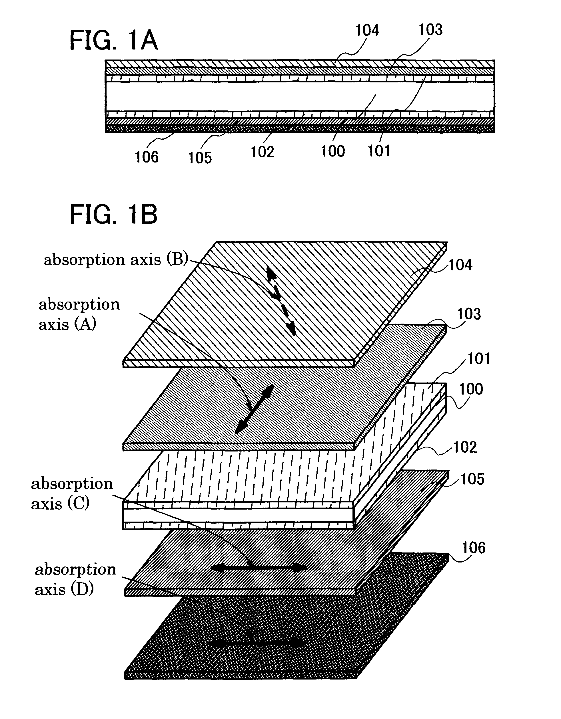
[0062]FIG. 1A is a cross-sectional view of a display device having a pair of stacked layers each including a polarizer, in which the wave length distributions of the extinction coefficients with respect to the absorption axes are different, and a structure in which at least one of the layers having the polarizers is disposed so as to be deviated from a parallel Nicols state. FIG. 1B is a perspective view of the display device. In this embodiment mode, an example of a liquid crystal display device having a liquid crystal element as a display element will be described.

[0063]As shown in FIG. 1A, a layer 100 having a liquid crystal element is sandwiched between a first substrate 101 and a second substrate 102 which are arranged so as to face each other.

[0064]In this embodiment mode, stacked layers each includi...

embodiment mode 2

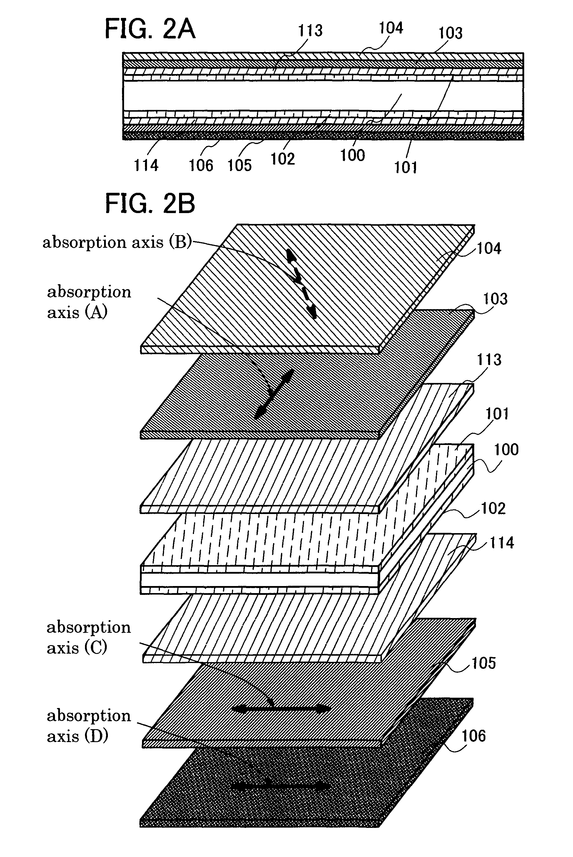
[0077]This embodiment mode will describe a concept of a display device provided with a retardation plate in addition to a pair of stacked layers each including a polarizing plate having a different wavelength distribution of extinction coefficient from each other with respect to the absorption axes unlike the above embodiment mode.

[0078]FIG. 2A is a cross-sectional view of a display device in which one of the pair of stacked layers each including a polarizer having a different wavelength distribution of extinction coefficient from each other with respect to the absorption axis is stacked to be deviated from a parallel Nicols state, and retardation plates are provided between the pair of stacked layers each including a polarizer and substrates respectively, while FIG. 2B is a perspective view of the display device. In this embodiment mode, a liquid crystal display device having a liquid crystal element as a display element will be explained as an example.

[0079]As shown in FIG. 2A, a ...


PUM


Abstract

To provide a display device having a high contrast ratio by a simple and easy method and to manufacture a high-performance display device at low cost, in a display device having a display element between a pair of light-transmitting substrates, layers each including a polarizer having different wavelength distribution of extinction coefficient from each other with respect to the absorption axes are stacked and provided on an outer side of the light-transmitting substrates. Further, a retardation plate may be provided between the stacked polarizers.

Description

BACKGROUND OF THE INVENTION[0001]1. Field of the Invention[0002]The present invention relates to a structure of a display device having a polarizer.[0003]2. Description of the Related Art[0004]A so-called flat panel display, which is a display device that is very thin and lightweight as compared to the conventional cathode-ray tube display device, has been developed. A liquid crystal display device having a liquid crystal element as a display element, a light emitting device having a self-light emitting element, an FED (field emission display) using an electron beam, and the like compete in the market of flat panel displays. Therefore, lower power consumption and a higher contrast ratio are demanded to increase the added value so as to differentiate from other products.[0005]In general, in a liquid crystal display device, each substrate is provided with one polarizing plate to keep a contrast ratio. When display of darker black is performed, the contrast ratio can be increased accor...

Claims


Application Information

Patent Timeline
IPC IPC(8): G02F1/1335
CPCG02F1/133533G02F1/13363G02F2203/64G02F2203/04G02F2001/133531G02F1/133531G02B5/30G02F1/1335
Inventor EGI, YUJIISHITANI, TETSUJINISHI, TAKESHI
Owner SEMICON ENERGY LAB CO LTD
Why Eureka
Try Eureka