Semiconductor substrate cleaning method and semiconductor substrate cleaning machine

a technology of semiconductor substrate and cleaning method, which is applied in the direction of cleaning equipment, cleaning equipment, chemical instruments and processes, etc., to achieve the effect of enhancing the performance of removing the particles from the surface of the semiconductor substrate, reducing the re-adhesion of the particles, and cleaning at high cleanliness

Inactive Publication Date: 2007-08-09
RENESAS TECH CORP +1
View PDF6 Cites 13 Cited by
  • Summary
  • Abstract
  • Description
  • Claims
  • Application Information

AI Technical Summary

Benefits of technology

[0051]Either arrangement suppresses re-adhesion of the particles detached from the surface of the semiconductor substrate by the first cleaning to the surface thereof (recontamination of the surface of the semiconductor substrate), and the performance of removing the particles from the surface of the semiconductor substrate is enhanced.
[0052]As described above, in the semiconductor substrate cleaning method and the semiconductor substrate cleaning machine according to the present invention, cleaning is performed while the particles once detached from the surface of the semiconductor substrate is prevented from adhering again to the surface thereof, thereby removing the particles from the semiconductor substrate. Hence, cleaning at high cleanliness is enabled, and accordingly, brush cleaning of the semiconductor substrate can be performed excellently. The present invention necessitates no considerable modification of a conventional cleaning machine, and therefore, can be realized effortlessly at low cost.

Problems solved by technology

Brush cleaning, however, involves the following problems.

Method used


Image

  • Semiconductor substrate cleaning method and semiconductor substrate cleaning machine
  • Semiconductor substrate cleaning method and semiconductor substrate cleaning machine
  • Semiconductor substrate cleaning method and semiconductor substrate cleaning machine

Examples


embodiment 1

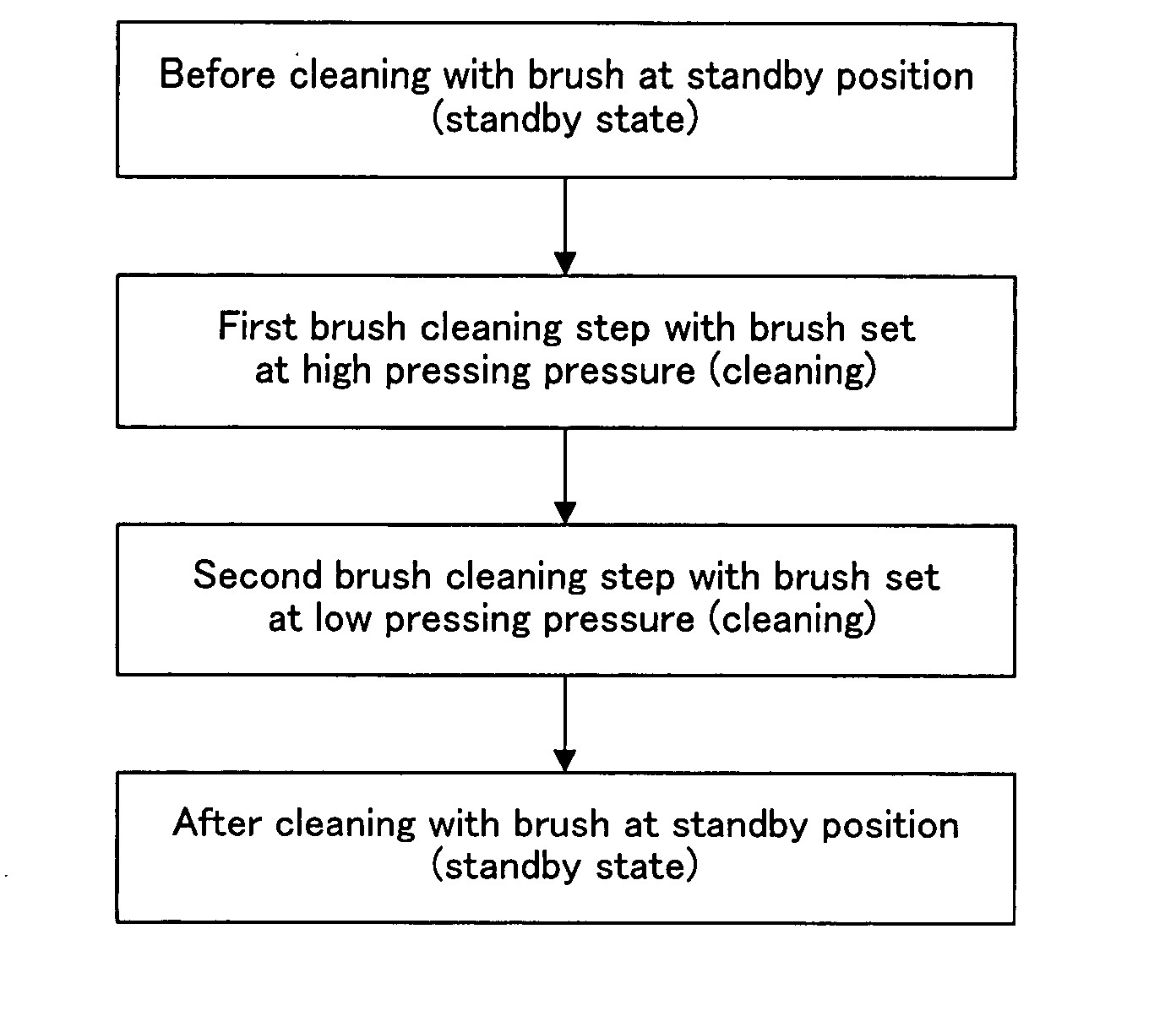
[0083]A semiconductor substrate cleaning method and a semiconductor substrate cleaning machine according to Embodiment 1 of the present invention will be described hereinafter with reference to the drawings.

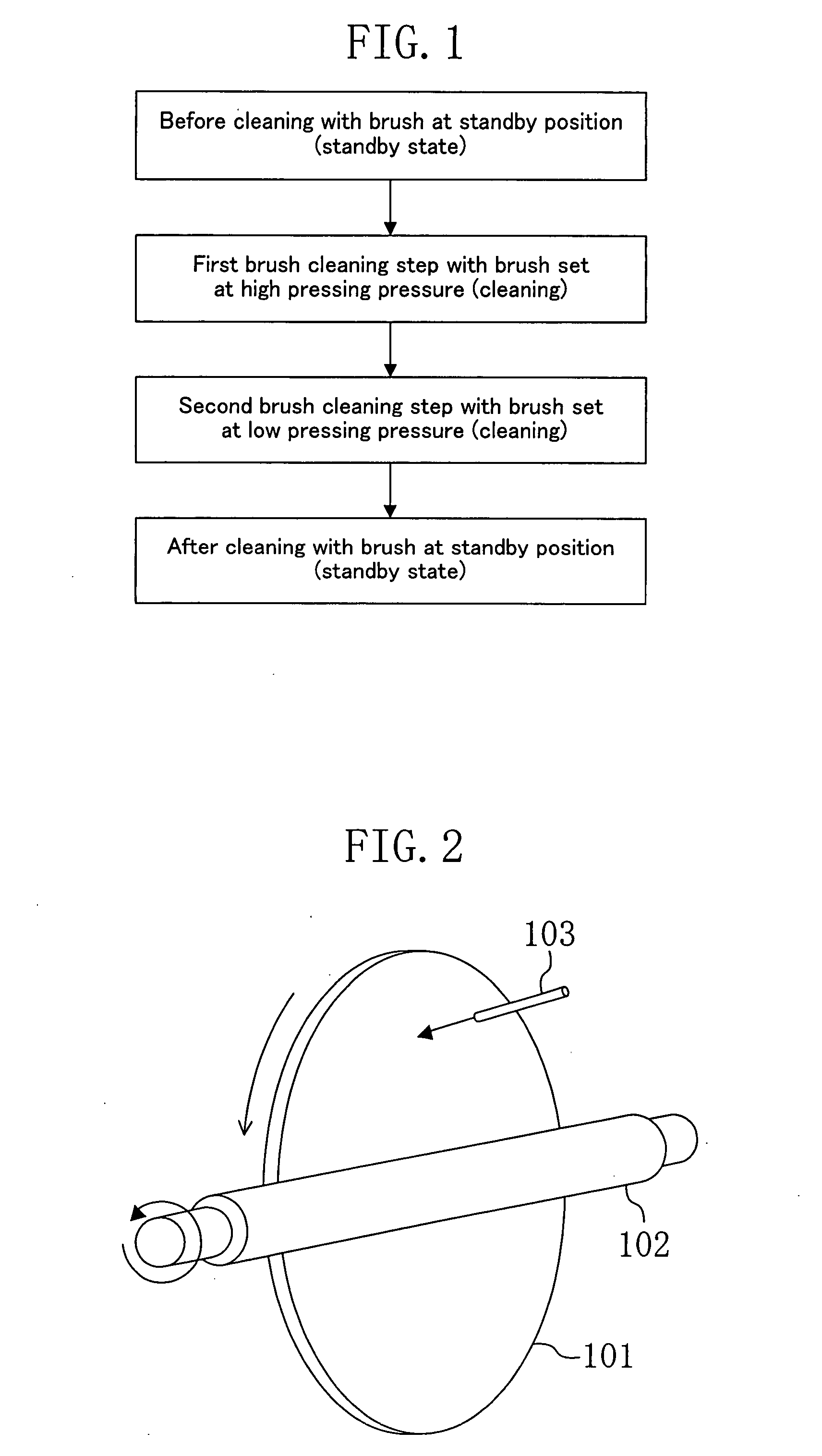
[0084]FIG. 1 is a flowchart depicting a flow of the semiconductor substrate cleaning method according to the present embodiment. As depicted in FIG. 1, in the semiconductor substrate cleaning method of the present embodiment, the flow starts from a standby state before cleaning, proceeds to first brush cleaning and second brush cleaning for respective predetermined time periods, and then, terminates. In the second brush cleaning step, a pressing pressure of a brush is set lower than that in the first brush cleaning, so that particles can be removed with re-adhesion of the particles to the surface of a semiconductor substrate (recontamination of the surface of the semiconductor substrate) suppressed by suppressing generation of static electricity. The term “high pressing pressure ...

embodiment 2

[0102]A semiconductor substrate cleaning method and a semiconductor substrate cleaning machine according to Embodiment 2 will be described below with reference to the drawings.

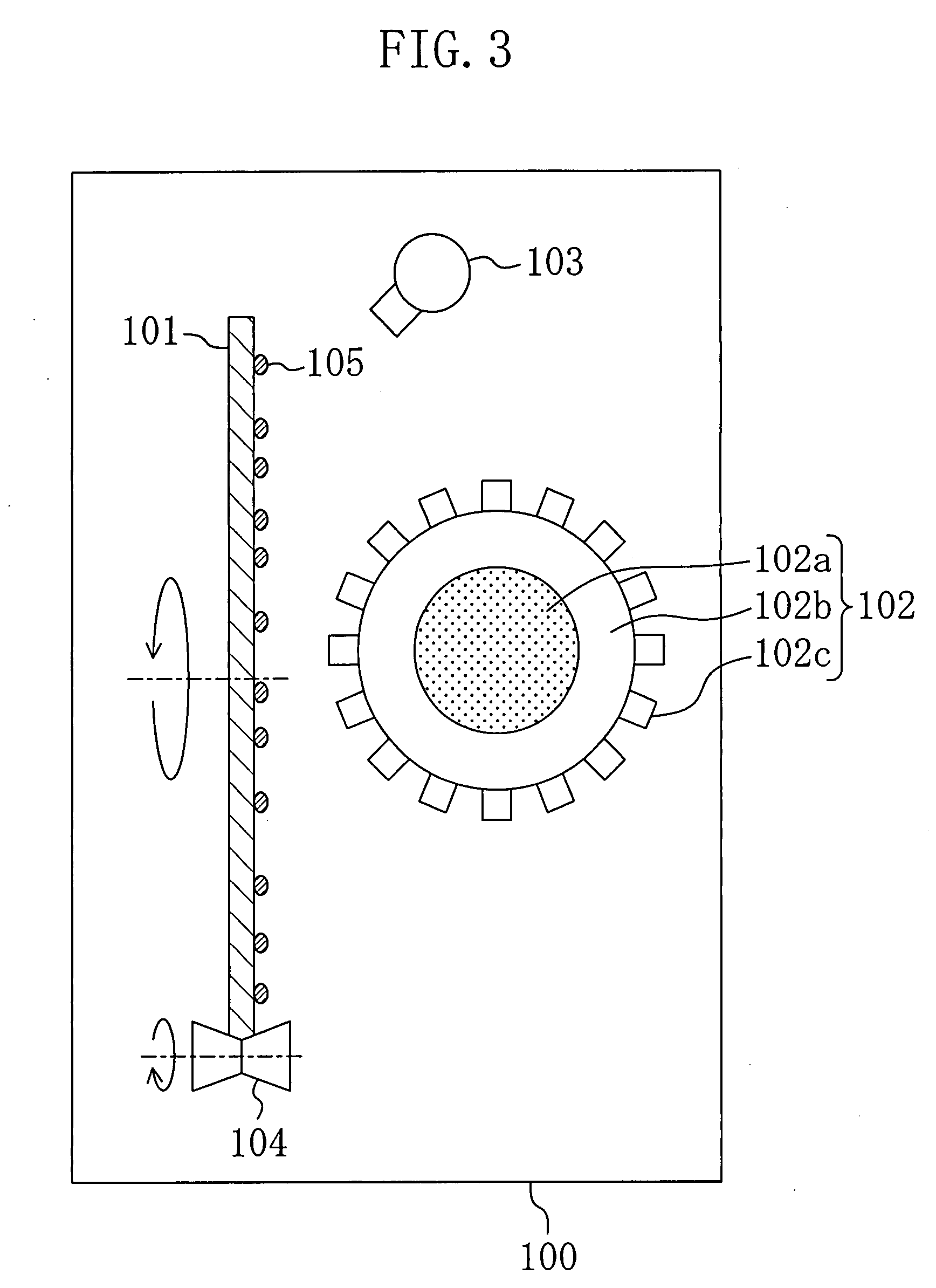
[0103]FIG. 6 is a flowchart depicting a flow of the semiconductor substrate cleaning method according to Embodiment 2. The semiconductor substrate cleaning method of the present embodiment includes, similarly to the semiconductor substrate cleaning method of Embodiment 1 depicted in FIG. 1, a first brush cleaning step and a second brush cleaning step which are performed for respective predetermined time periods. In contrast to Embodiment 1 in which the second brush cleaning step is performed with the pressing pressure of the brush changed from that in the first brush cleaning step, the second brush cleaning step is performed with the position of the brush relative to the semiconductor substrate changed from that in the first brush cleaning step. Specifically, in the second brush cleaning step, the brush is set...

embodiment 3

[0116]A semiconductor substrate cleaning method and a semiconductor substrate cleaning machine according to Embodiment 3 will be described below with reference to the drawings.

[0117]FIG. 9 is a flowchart depicting a flow of the semiconductor substrate cleaning method according to Embodiment 3. The semiconductor substrate cleaning method of the present embodiment includes, similarly to the semiconductor substrate cleaning methods of Embodiments 1 and 2, a first brush cleaning step and a second brush cleaning step which are performed for respective predetermined time periods. Wherein, in the present embodiment, cylindrical brushes having different diameters are prepared and exchanged between the first and second brush cleaning steps. Specifically, the outer diameter of a cylindrical brush used in the second brush cleaning step is set smaller than that in the first brush cleaning step. The term “large outer diameter and small outer diameter” in FIG. 9 implies relative sizes of the brus...


PUM

PropertyMeasurementUnit
outer diameter D2aaaaaaaaaa
height H2aaaaaaaaaa

Abstract

A semiconductor substrate cleaning method includes a first cleaning step of cleaning the surface of a semiconductor substrate with the use of a first brush and a second cleaning step of cleaning the surface of the semiconductor substrate with the use of a second brush after the first cleaning step. The second cleaning step is performed under a condition that suppresses recontamination of the surface of the semiconductor substrate in comparison with the first cleaning step.

Description

CROSS REFERENCE TO RELATED APPLICATIONS[0001]This Non-provisional application claims priority under 35 U.S.C. § 119(a) on Patent Application No. 2006-31508 filed in Japan on Feb. 8, 2006, the entire contents of which are hereby incorporated by reference.FIELD OF THE INVENTION[0002]The present invention relates to a semiconductor substrate cleaning method by which particles on a semiconductor substrate are reduced by removing particles efficiently and preventing re-adhesion of the removed particles to the semiconductor substrate.BACKGROUND ART[0003]As a method for removing particles adhering to the surface of a semiconductor substrate, brush cleaning may be employed. In the brush cleaning, particles are removed by a combination of lift-off action, electrical repulsion and the like of a cleaning solution and physical action by friction of a brush.[0004]In the conventional brush cleaning of a semiconductor substrate, a semiconductor substrate is driven and rotated while a brush is move...

Claims


Application Information

Patent Timeline
Patent Type & Authority Applications(United States)
IPC IPC(8): C23G1/00B08B7/00
CPCB08B1/04H01L21/67046H01L21/02074B08B3/02
Inventor KOBAYASHI, KENJIOSHITA, HIROSHI
Owner RENESAS TECH CORP
Why Eureka
Try Eureka