
Eureka
For R&D, Eureka makes reading and utilizing patents & technical documents easy.
Eureka AIR
Designed for self-driven R&D workflows. Generate viable solutions, solve complex R&D challenges, empower your innovation with AI.

Eureka Materials
Designed for material experts only. Revolutionize your material R&D, from search, analyze, to developing new materials.

TechResearch
Generate reliable direction feasibility study reports for your R&D in just a few steps.

TechSeek
Discover and master advanced knowledge NOW. Basics, ideas, possibilities, all at once.

TechMind
As an expert in R&D Theories, TechMind can generates customized viable solutions instantly.

TechRisk
Analyze your overall solution with one click, know your potential R&D risks in advance.

TechMonitor
Get weekly tech updates, stay abreast of the latest tech innovations and key insights.
Substrate and method for mounting silicon device
- Summary
- Abstract
- Description
- Claims
- Application Information
AI Technical Summary
Benefits of technology
Problems solved by technology
Method used
Image

Examples
Embodiment Construction
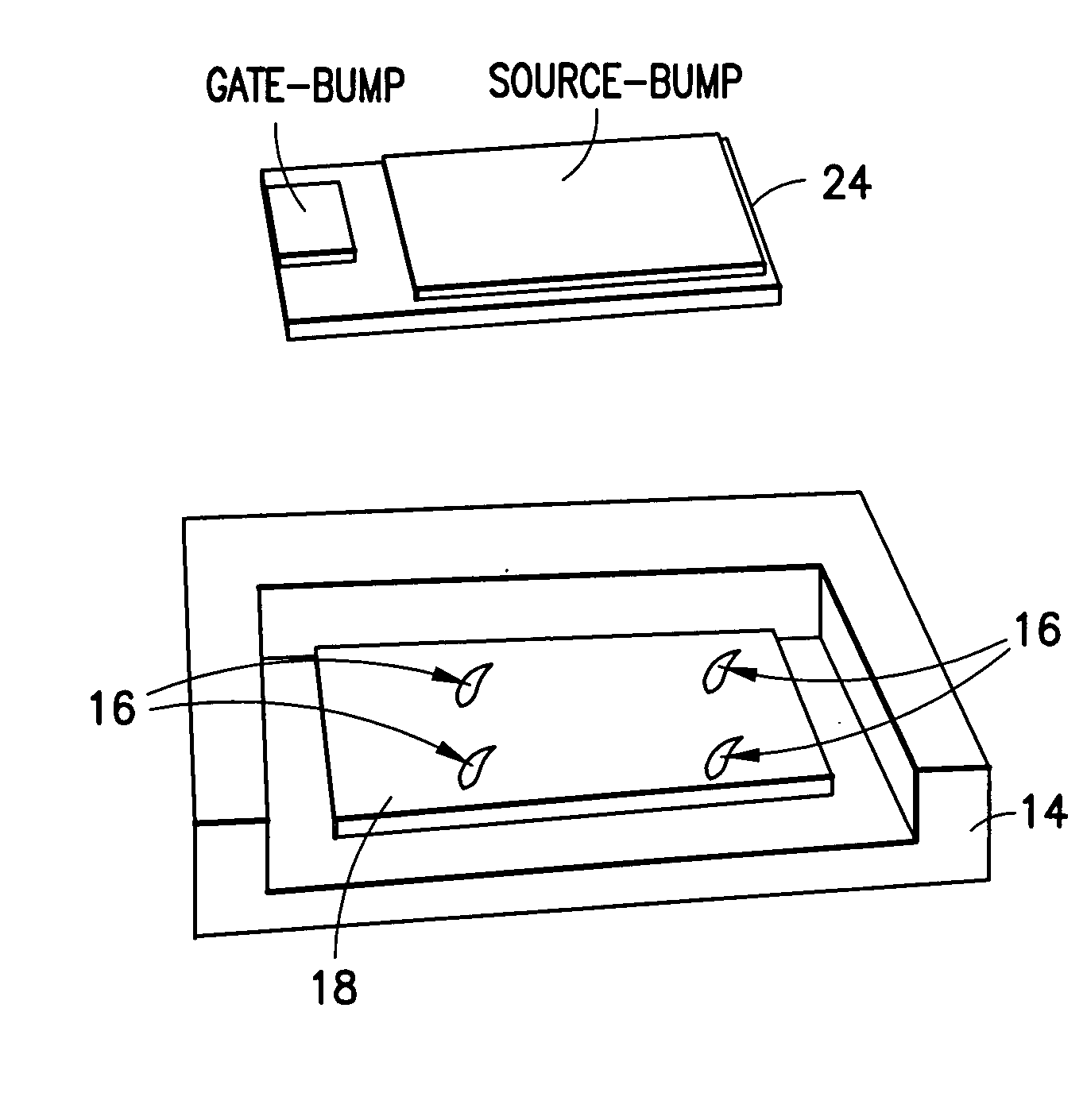
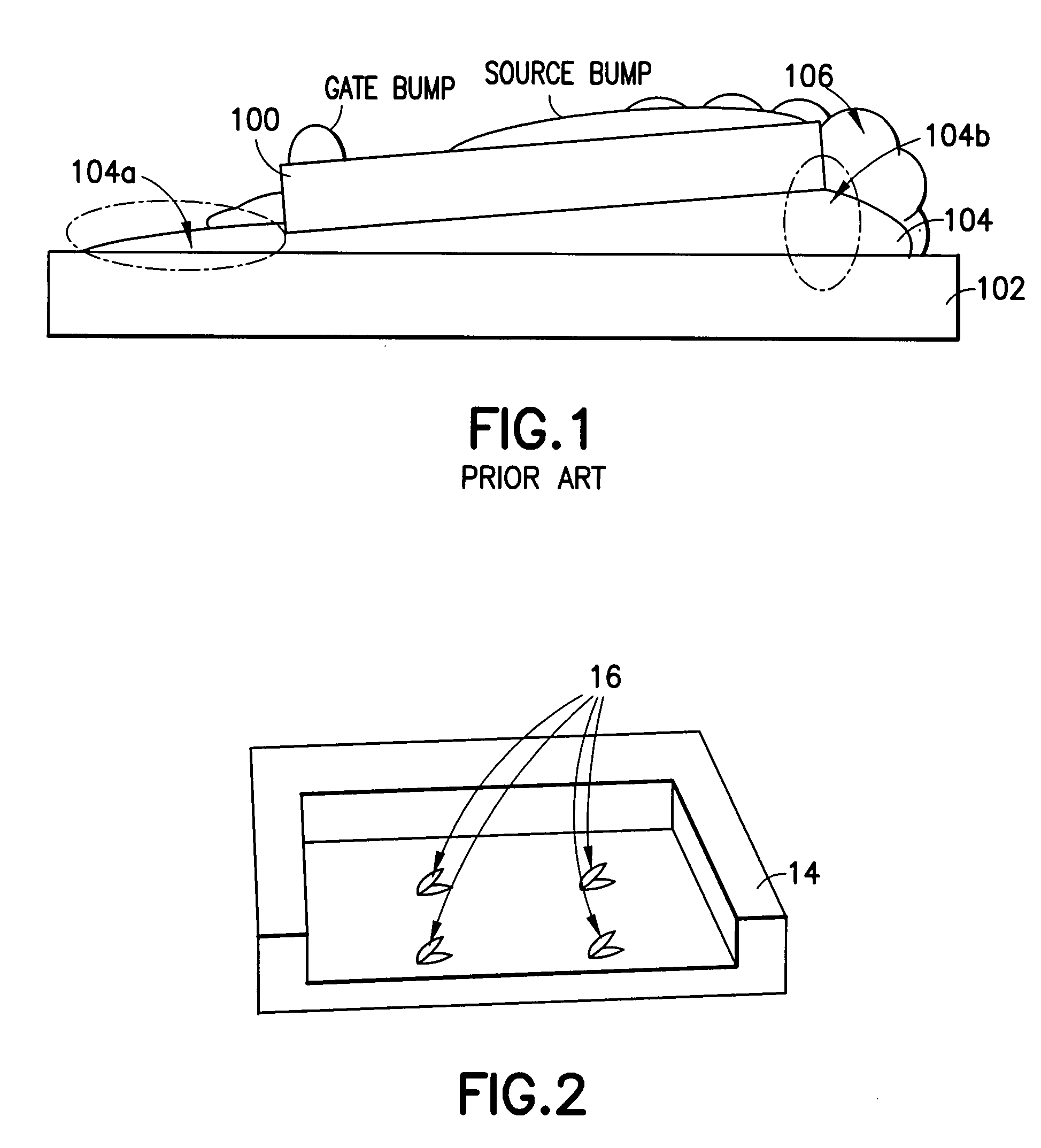
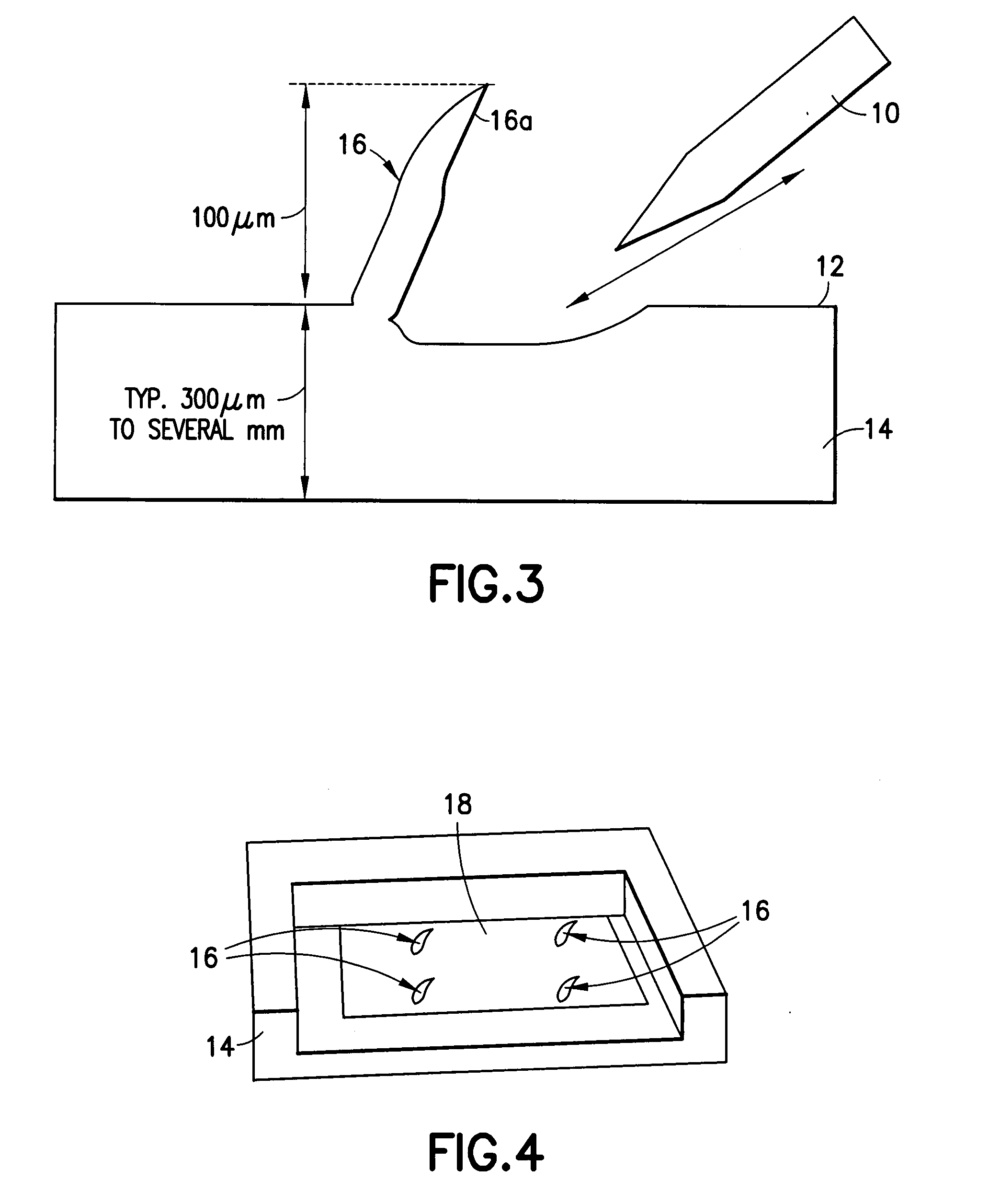
[0031] A substrate on which a Si-device, or die is mounted in accordance with an embodiment of the present invention is illustrated, for example, in FIGS. 2-6 of the present application. In a preferred embodiment, as illustrated in FIG. 3, a needle-like tool 10 is used to gouge the top metal surface 12 of the substrate 14 to produce a substantially vertical protrusion 16 (or swarf) extending upward from the surface 12 of the substrate 14. As illustrated, the protrusion 16 preferably has a height of approximately 100 μm. While this is a preferred height of the protrusion 16, the height of the protrusion may be modified as appropriate for the specific application.
[0032] In a preferred embodiment, the substrate 12 is a metallic can, for example the metal can utilized in the DirectFET® line of products or the Cu-layer of a horseshoe shaped DBC such as that described above in co-pending application entitled PACKAGE FOR HIGH POWER DENSITY DEVICES. However, the protrusions 16 may similarl...
PUM
 Abstract
Description
Claims
Application Information
 - R&D Engineer
- R&D Manager
- IP Professional
- Industry Leading Data Capabilities
- Powerful AI technology
- Patent DNA Extraction
Browse by: Latest US Patents, China's latest patents, Technical Efficacy Thesaurus, Application Domain, Technology Topic, Popular Technical Reports.
© 2024 PatSnap. All rights reserved.Legal|Privacy policy|Modern Slavery Act Transparency Statement|Sitemap|About US| Contact US: help@patsnap.com