Semiconductor device, wiring substrate forming method, and substrate processing apparatus

a semiconductor and substrate technology, applied in the direction of semiconductor/solid-state device manufacturing, electrical equipment, basic electric elements, etc., can solve the problems of high manufacturing cost, difficult scaling down, circuit damage, etc., and achieve easy and inexpensive high-speed planarization, easy fine control of thickness, and efficient removal of substrate

Inactive Publication Date: 2007-08-09
FUJITSU LTD
View PDF12 Cites 5 Cited by
  • Summary
  • Abstract
  • Description
  • Claims
  • Application Information

AI Technical Summary

Benefits of technology

[0014] The present invention is made in view of the aforementioned problems, and considering that it is mainly directed to machining other than CMP represented as a planarization method, variations in the thickness of a substrate (especially, a semiconductor substrate and a conductor / insulating substrate) are made uniform, and high-speed planarization is realized easily and inexpensively without disadvantages such as dishing and without any limitation on a wiring design. Moreover, an object of the present invention is to provide a wiring substrate forming method and a semiconductor device, and a substrate processing apparatus capable of, when a multilayer wiring thin film is obtained as a single body by finally removing the substrate, easily performing fine control of thicknesses of respective wiring layers composing the multilayer wiring thin film and removing the substrate efficiently at low cost to realize the wiring thin film having a fine wiring structure.

Problems solved by technology

This wiring substrate can be realized at low cost, but scaling down is difficult since the via diameter is approximately between 120 μm and 200 μm, L / S (Line / Space) is approximately between 100 μm / 100 μm and 200 μm / 200 μm.
Fine planarization can be realized if the CMP method is used, but its process requires a high manufacturing cost since a processing apparatus is expensive and throughput is low.
This stripping method is, so to speak, the image of stripping off a film, and has a possibility of causing damage to a circuit.
Even if either of these methods is adopted, the supporting base itself is reflected in cost, in addition, if the supporting base is a semiconductor substrate in the latter method, a residue after grinding all becomes rubbish, and an enormous amount of rubbish is produced through the process, so that a bad influence on the environment cannot be ignored.

Method used


Image

  • Semiconductor device, wiring substrate forming method, and substrate processing apparatus
  • Semiconductor device, wiring substrate forming method, and substrate processing apparatus
  • Semiconductor device, wiring substrate forming method, and substrate processing apparatus

Examples


specific embodiments

[0051] Based on the aforementioned basic gist, specific embodiments of the present invention will be described below using the drawings.

first embodiment

[0052] Here, a silicon semiconductor substrate (silicon wafer) is shown as an example of a substrate, and a case where a multilayer wiring formed by staking wirings in plural layers in an insulator is formed on the semiconductor substrate is disclosed.

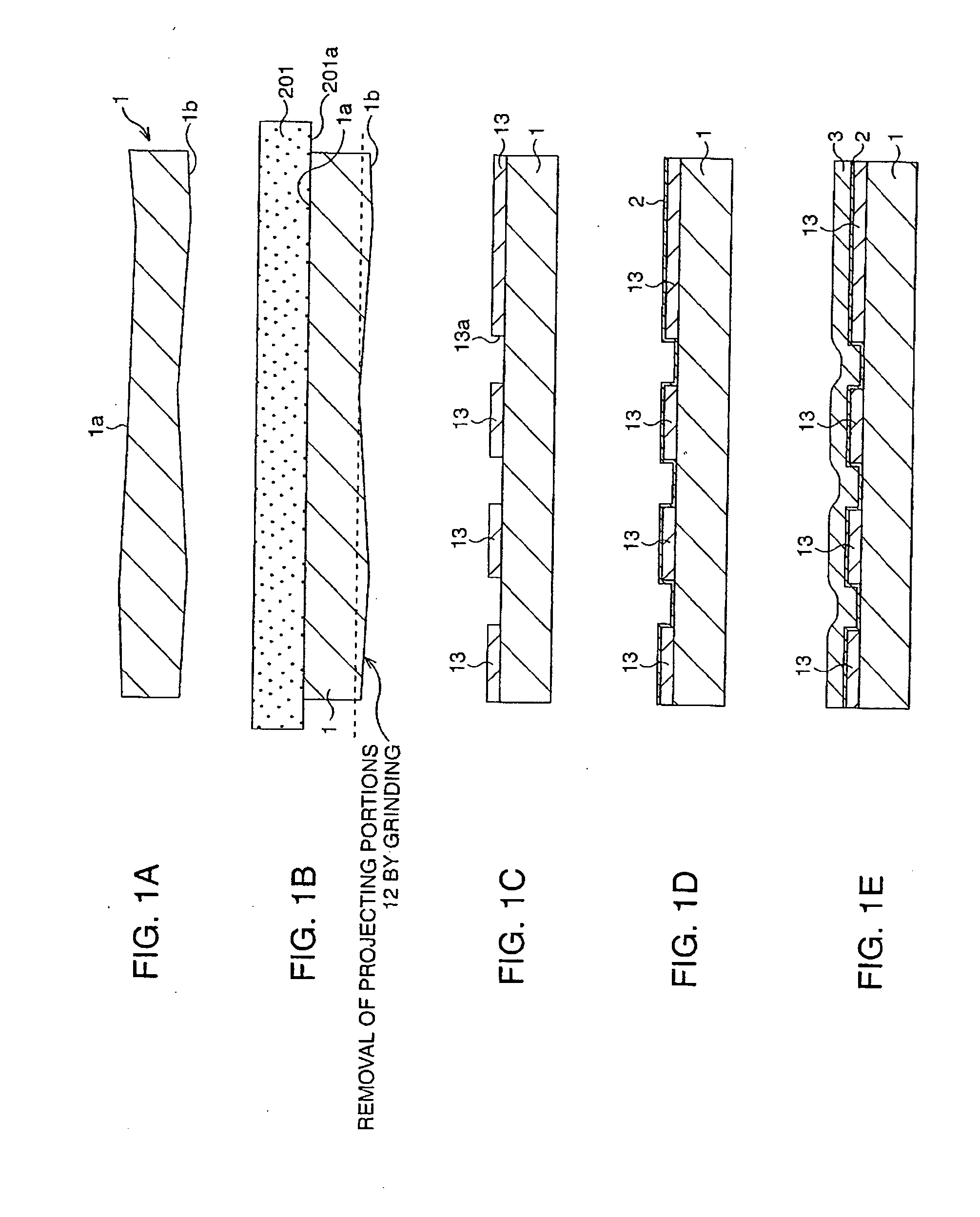
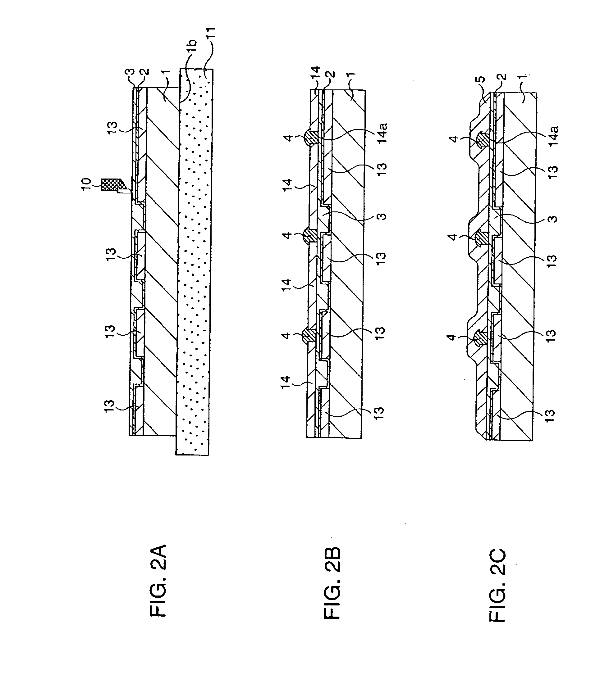
[0053]FIG. 1A to FIG. 1E, FIG. 2A to FIG. 2C, FIG. 3A to FIG. 3C, and FIG. 4A to FIG. 4C are schematic sectional views showing a multilayer wiring substrate forming method according to this embodiment step by step.

[0054] First, as shown in FIG. 1A, a silicon semiconductor substrate 1 is prepared. Usually, the silicon semiconductor substrate is not uniform in thickness as shown and besides has undulations.

[0055] Hence, as a preceding process to subject one principal surface of the semiconductor substrate 1, here a substrate front surface (wiring forming surface 1a), to cutting with a tool which will be described later, the other principal surface of the semiconductor substrate 1, here a back surface 1b (of the wiring forming surface ...

second embodiment

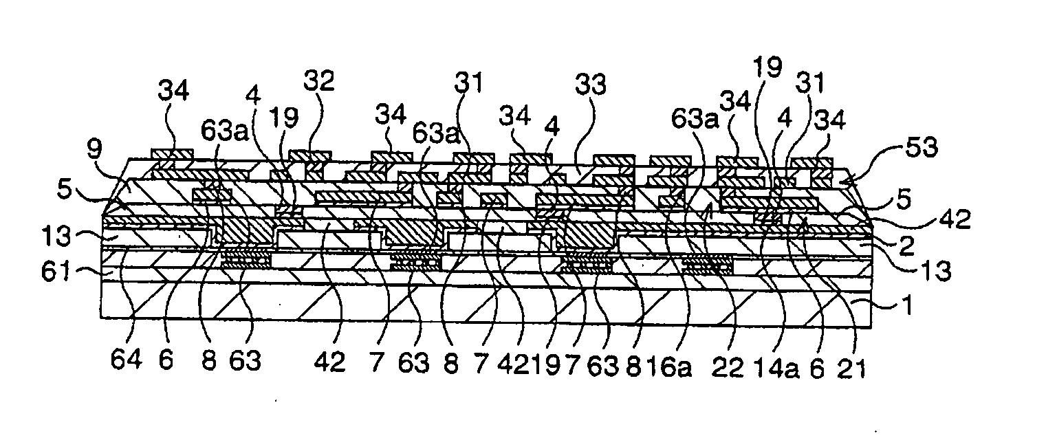
[0110] Here, a silicon semiconductor substrate is shown as an example of a substrate, and a case where a multilayer wiring layer formed by stacking a plurality of wiring layers each composed of wirings in an insulator is formed when an LSI is manufactured is disclosed.

[0111] Among semiconductor devices including a multilayer wiring layer are those which have forms such as shown in FIG. 13 and FIG. 14. In the semiconductor device in FIG. 13, electrodes 63a are formed so as to surround a periphery of an element region 302 where plural (many) semiconductor elements (MOS transistors or the like) are formed in a silicon semiconductor substrate 301, and the respective semiconductor elements and the electrodes 63a are electrically connected. On the other hand, in the semiconductor device in FIG. 14, plural electrodes 63a are formed in matrix in the semiconductor substrate 301, and plural (many) semiconductor elements are formed between the electrodes 63a. Namely, in the case of FIG. 14, r...


PUM


Abstract

A substrate support (201) having a flat supporting surface (201a) is prepared, and a semiconductor substrate (1) is fixed to the substrate supporting surface (201) by attaching a wiring forming surface (1a) to the supporting surface (201a) by suction, for example, by vacuum suction. On this occasion, the wiring forming surface (1a) is forcibly flattened by being attached to the supporting surface (201a) by suction, and therefore the wiring forming surface (1a) becomes a reference plane for planarization of a back surface (1b). In this state, planarization processing is performed by mechanically grinding the back surface (1b) to grind away projecting portions (12) of the back surface (1b). Hence, variations in the thickness of the substrate (especially, semiconductor substrate) are made uniform, and high-speed planarization is realized easily and inexpensively without disadvantages such as dishing and without any limitation on a wiring design.

Description

CROSS-REFERENCE TO RELATED APPLICATIONS [0001] This application is the division of U.S. application Ser. No. 11 / 097,937 filed on Apr. 1, 2005, which is a continuation of PCT / JP03 / 15808 filed on Dec. 10, 2003 and claims the benefit of priority from the prior Japanese Patent Application No. 2002-358536, filed on Dec. 10, 2002, and PCT International Application No. PCT / JP03 / 06382, filed on May 22, 2003, the entire contents of which are incorporated herein by reference.TECHNICAL FIELD [0002] The present invention relates to a method of forming a multilayer wiring with an electronic device such as an LSI on a substrate, especially a semiconductor substrate, further a method of forming a multilayer wiring film by forming a multilayer wiring layer on a supporting base made of a metal material or an insulating material and removing the supporting base, a semiconductor device having a multilayer wiring, and a substrate processing apparatus. BACKGROUND ART [0003] Recently, with an increase in...

Claims


Application Information

Patent Timeline
Patent Type & Authority Applications(United States)
IPC IPC(8): H01L21/4763H01L21/3105H01L21/321H01L21/44H01L21/48H01L21/68H01L21/768
CPCH01L21/31058H01L21/32115H01L21/7684H01L21/4857H01L21/6835H01L21/4846
Inventor NAKAGAWA, KANAEMIZUKOSHI, MASATAKATESHIROGI, KAZUO
Owner FUJITSU LTD
Why Eureka
Try Eureka