Implant free extremely thin semiconductor devices

a technology of ultra-thin semiconductors and semiconductor devices, applied in the field of extremely thin silicononinsulator field-effect transistors, can solve the problems of difficult recrystallization of amorphous semiconductor layers, increased resistance of semiconductor devices, and difficult challenges, and achieve good thickness control across the wafer

Active Publication Date: 2012-11-06
TAIWAN SEMICON MFG CO LTD
View PDF11 Cites 9 Cited by
  • Summary
  • Abstract
  • Description
  • Claims
  • Application Information

AI Technical Summary

Benefits of technology

[0009]Epitaxially growing the extremely thin semiconductor layer on the Ge layer ensures good thickness control across the wafer. This process could be used for SOI or bulk wafers.

Problems solved by technology

ETSOI devices have very substantial advantages, however they also present difficult challenges.
Recrystallizing the amorphous semiconductor layer is difficult, because of the limited amount of crystal seed layer that is available in semiconductor layers having a thickness of less than 10 nm that have been ion implanted into an amorphous crystal structure.
Further, the resistance of the semiconductor device is increased by defects in the semiconductor layer that are produced by ion implantation.
The ion implantation may also damage the gate dielectric.

Method used


Image

  • Implant free extremely thin semiconductor devices
  • Implant free extremely thin semiconductor devices
  • Implant free extremely thin semiconductor devices

Examples


Embodiment Construction

[0022]Detailed embodiments of the present invention are disclosed herein; however, it is to be understood that the disclosed embodiments are merely illustrative of the invention that may be embodied in various forms. In addition, each of the examples given in connection with the various embodiments of the invention is intended to be illustrative, and not restrictive. Further, the figures are not necessarily to scale, some features may be exaggerated to show details of particular components. Therefore, specific structural and functional details disclosed herein are not to be interpreted as limiting, but merely as a representative basis for teaching one skilled in the art to variously employ the present invention.

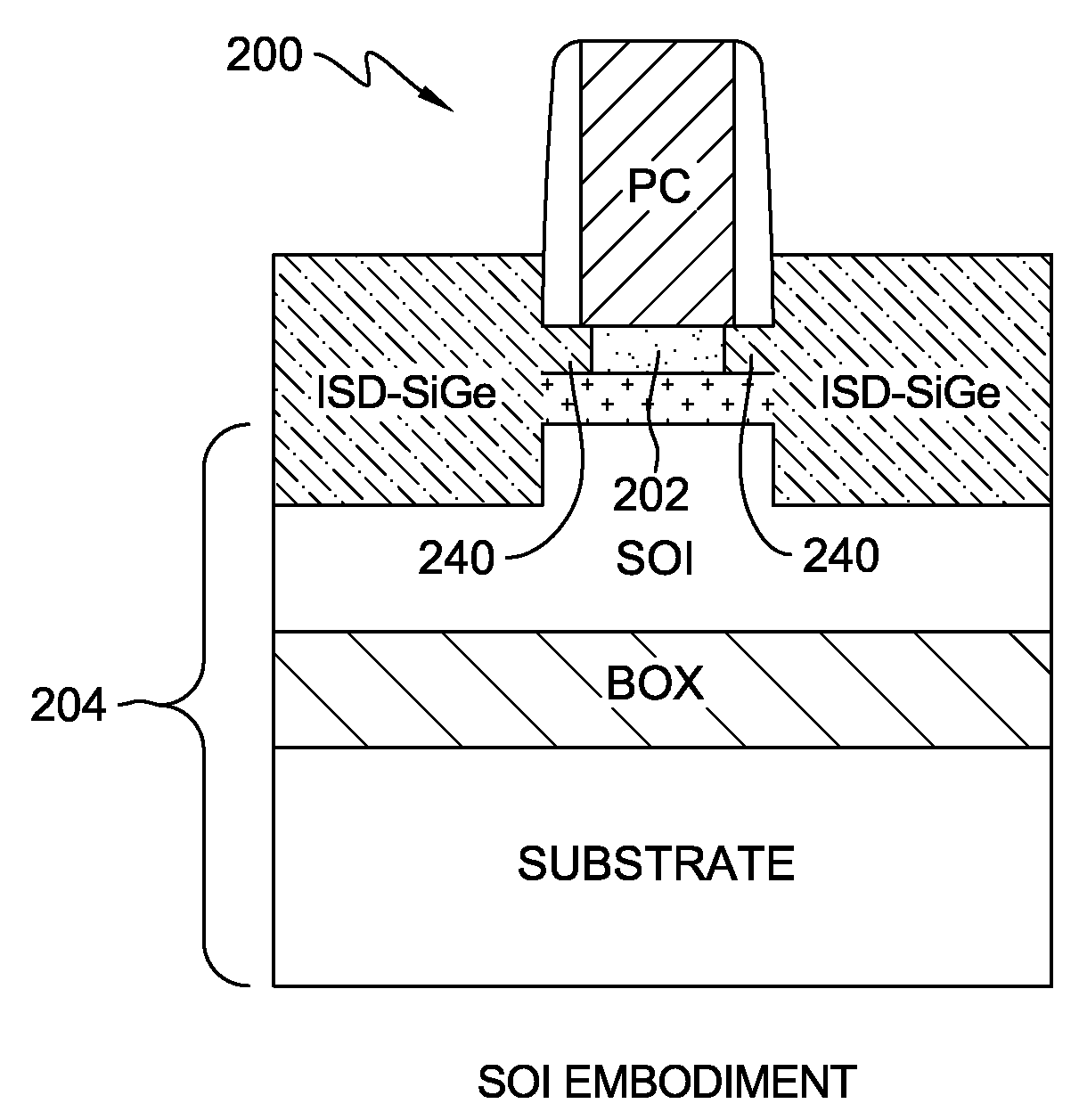
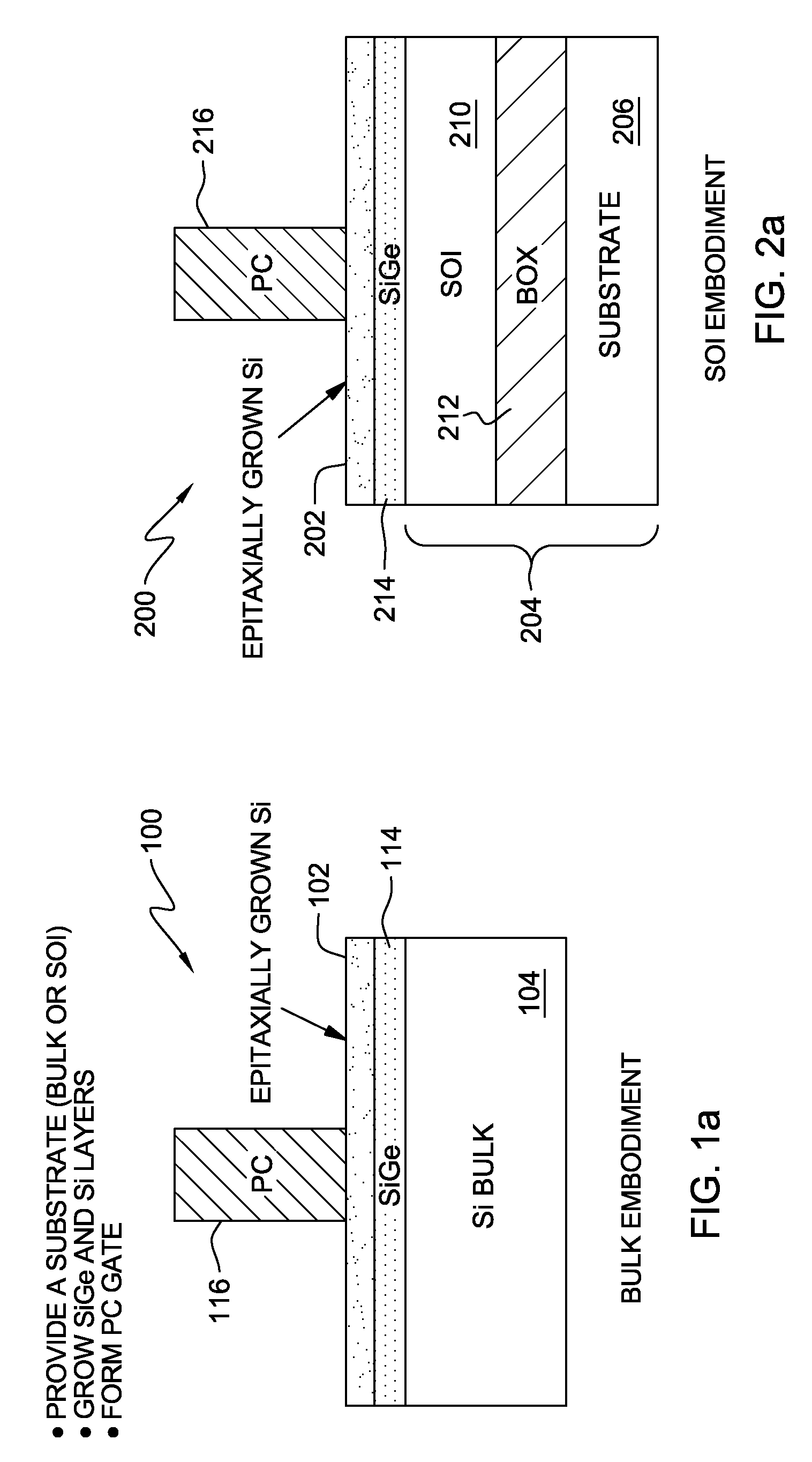
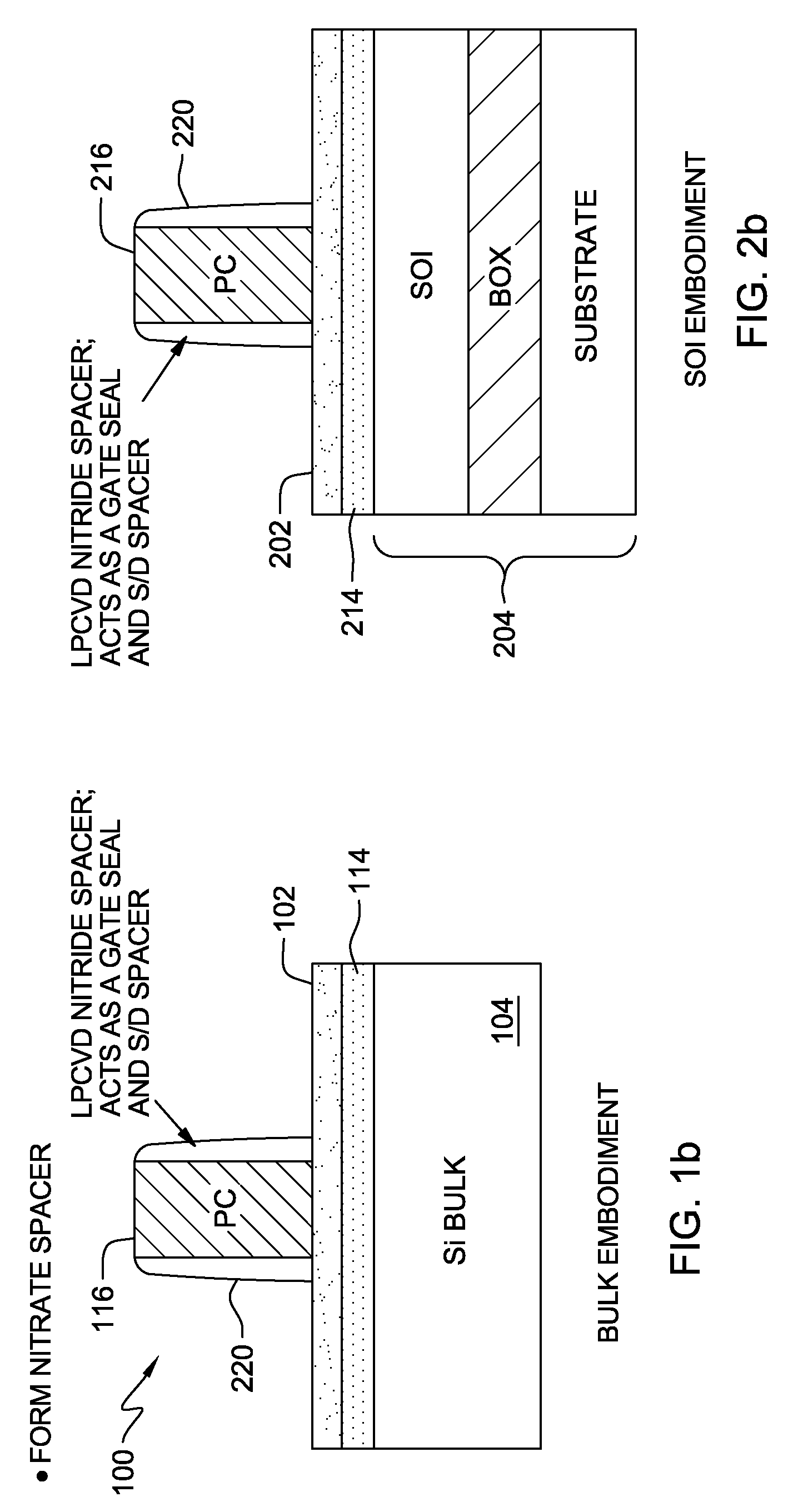
[0023]In one embodiment, the present invention relates to a method for forming a planar semiconductor device on a semiconductor on insulator (SOI) substrate having an extremely thin semiconductor on insulator (ETSOI) layer. An extremely thin semiconductor on insulator (ETSOI)...


PUM


Abstract

A semiconductor device and a method of fabricating a semiconductor device are disclosed. In one embodiment, the method comprises providing a semiconductor substrate, epitaxially growing a Ge layer on the substrate, and epitaxially growing a semiconductor layer on the Ge layer, where the semiconductor layer has a thickness of 10 nm or less. This method further comprises removing at least a portion of the Ge layer to form a void beneath the Si layer, and filling the void at least partially with a dielectric material. In this way, the semiconductor layer becomes an extremely thin semiconductor-on-insulator layer. In one embodiment, after the void is filled with the dielectric material, in-situ doped source and drain regions are grown on the semiconductor layer. In one embodiment, the method further comprises annealing said source and drain regions to form doped extension regions in the semiconductor layer. Epitaxially growing the extremely thin semiconductor layer on the Ge layer ensures good thickness control across the wafer. This process could be used for SOI or bulk wafers.

Description

BACKGROUND OF THE INVENTION[0001]1. Field of the Invention[0002]The present invention generally relates to the field of semiconductors, and more particularly relates to extremely-thin silicon-on-insulator field-effect transistors having extremely-thin silicon layers, and a method of fabricating the same.[0003]2. Background Art[0004]In order to be able to make integrated circuits (ICs), such as memory, logic, and other devices, of higher integration density than currently feasible, one has to find ways to further downscale the dimensions of field effect transistors (FETs), such as metal-oxide-semiconductor field effect transistors (MOSFETs) and complementary metal oxide semiconductors (CMOS). Scaling achieves compactness and improves operating performance in devices by shrinking the overall dimensions and operating voltages of the device while maintaining the device's electrical properties. Additionally, all dimensions of the device must be scaled simultaneously in order to optimize ...

Claims


Application Information

Patent Timeline
Patent Type & Authority Patents(United States)
IPC IPC(8): H01L21/00H01L21/84
CPCH01L29/66636H01L29/78654H01L29/66772H01L29/78621
Inventor CHENG, KANGGUODORIS, BRUCE B.GUO, DECHAOKULKARNI, PRANITAOLDIGES, PHILIP J.SHAHIDI, GHAVAM G.
Owner TAIWAN SEMICON MFG CO LTD
Why Eureka
Try Eureka