Method of manufacturing a bulk acoustic wave device

a technology of acoustic waves and bulk acoustic waves, which is applied in the manufacture/assembly of piezoelectric/electrostrictive devices, electrical equipment, cable/conductor manufacturing, etc., can solve problems such as difficulty in achieving, and achieve the effect of reducing insertion loss, increasing the quality factor of said desired eigenmode, and achieving the effect of dispersion characteristics in the electrode region

Active Publication Date: 2011-12-29
VLSI TECH LLC
View PDF3 Cites 9 Cited by
  • Summary
  • Abstract
  • Description
  • Claims
  • Application Information

AI Technical Summary

Benefits of technology

[0020]In this case, when planarization is completed, the height of the top surface of the dielectric is equal to the sum of the electrode thickness and the stop-layer thickness. Thus, the thickness of the dielectric layer is determined by the sum of the thicknesses of the electrode and stop-layer. It is brought to its final thickness by the planarization process, instead of the process of depositing the dielectric. This may give enhanced control of thickness. The difference in height between the electrode portion and remaining portion is determined by the thickness of the stop-layer. It is preferable that the stop-layer is relatively hard, so that it is not partially removed by the planarization. This will ensure that the end point of the planarization process—and therefore the thickness of the dielectric layer—is determined accurately.
[0022]The present inventors have identified another problem of conventional BAW manufacturing methods, which also leads to poor control of layer thicknesses. When patterning the electrode on the active layer, part of the active layer itself may be removed. This causes the thickness of the device in the remaining portion (the portion around the electrode) to be changed by an unknown amount. The present processing method can reduce this unwanted variation, by patterning the electrode in two steps. The first step is an anisotropic (directional) etching step, such as dry plasma etching. The first etching step does not expose the underlying active layer, but leaves a thin layer of the conductive layer intact. The second etching step is isotropic (non-directional). The etchant (for example, chlorine gas) will etch the conductive material more selectively in the isotropic mode. Therefore, there is less likelihood of significant, unintended etching of the active layer.
[0025]This can allow more precise control of the dispersion characteristics, because both the thicknesses of layers and their acoustic properties can be controlled. Acoustic impedance is related to the density of a material.
[0028]The Bulk Acoustic Wave device may be adapted for acoustic coupling of signals at frequencies in a desired pass-band, and a thickness of the first dielectric layer in the remaining portion may be adapted such that the wave number for at least one desired eigenmode having an eigenfrequency within the pass-band is an imaginary number, so as to increase the quality factor of said desired eigenmode and reduce insertion loss in the pass-band.
[0029]By designing the device to have this dispersion characteristic, the layer stack of the device is adapted so that the desired eigenmode is trapped by the remaining portion (the external region around the electrode). This provides improved pass-band characteristics when the BAW device is used as a filter.
[0033]This provides an additional degree of freedom in the device design. The layer structure of the gap can be made different to that of the remaining portion of the device. This can lead to enhanced bandwidth of the pass-band.

Problems solved by technology

However, this is difficult to achieve—especially if the electrode is relatively soft compared with the dielectric.

Method used


Image

  • Method of manufacturing a bulk acoustic wave device
  • Method of manufacturing a bulk acoustic wave device
  • Method of manufacturing a bulk acoustic wave device

Examples


Embodiment Construction

[0065]The design of vertically-coupled BAW filters is relatively straightforward. The required inter-resonator coupling-strengths can be calculated from standard filter theory. Once these parameters are known, one-dimensional simulations can be used to design the layer stack of a device providing the required coupling. The lateral layout is then easily determined based on the required impedance.

[0066]Unfortunately, the realization of filters of this type is rather impractical. It is essential that the stacked resonators have a resonance frequency exactly matched to the desired filter frequency. Furthermore, vertical coupling necessarily requires many layers: at least two piezoelectric layers, as well as electrodes, and coupling layers (typically three). A more cost-effective alternative to vertical coupling is therefore desirable.

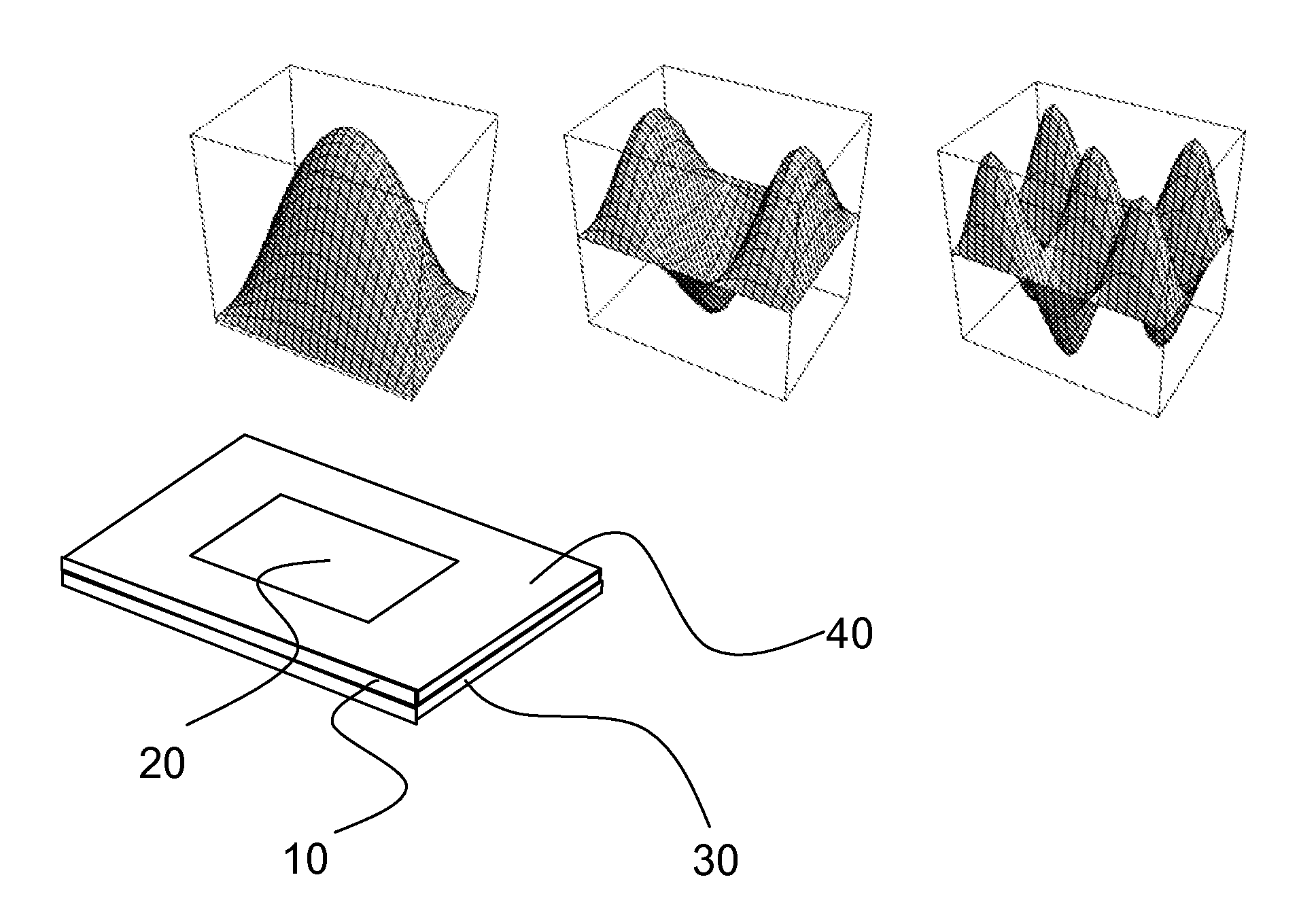
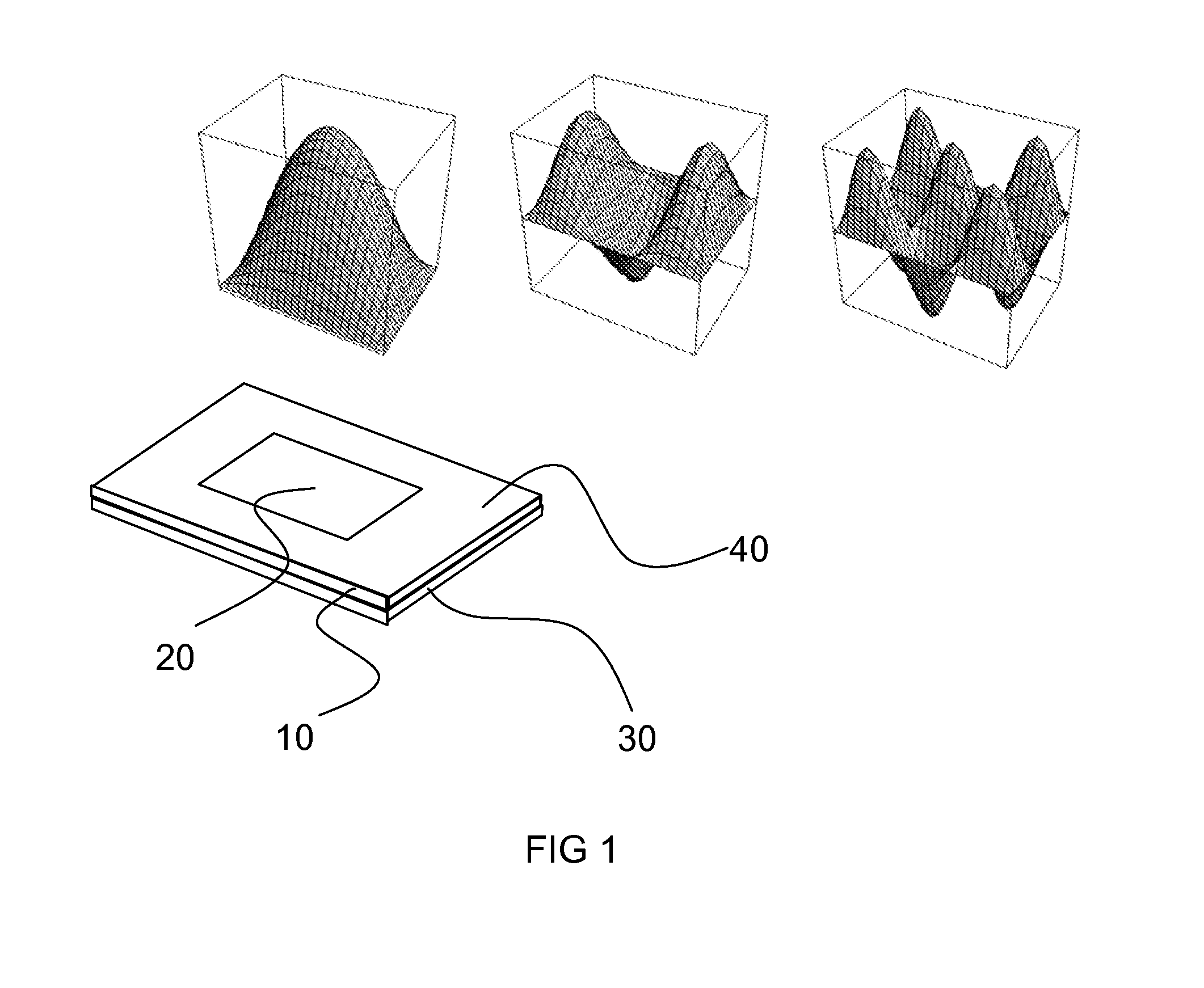
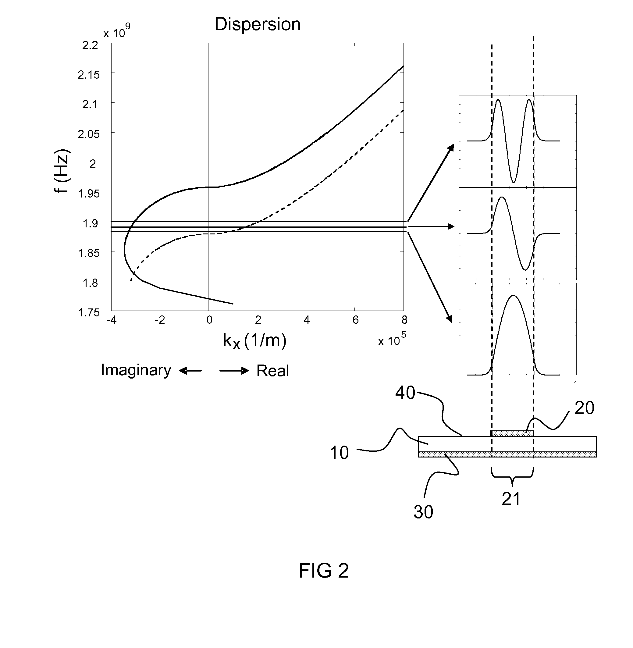
[0067]To avoid the problems associated with VBAW filters, embodiments of the current invention provide improved designs for laterally-coupled BAW filters. ...


PUM


Abstract

A method of manufacturing a Bulk Acoustic Wave device by providing an active layer formed of an electro-mechanical transducer material, providing a first electrode on the active layer, defining a first electrode portion of the device, whereby a remaining portion of the device is defined around the first electrode, providing a stop-layer on the first electrode, depositing a first dielectric layer on the resultant structure, and planarizing the first dielectric layer until the stop-layer on the first electrode is exposed.

Description

[0001]This application claims the priority under 35 U.S.C. §119 of European patent application no. 09179278.8, filed on Dec. 15, 2009, the contents of which are incorporated by reference herein.FIELD OF THE INVENTION[0002]This invention relates to methods for manufacturing bulk acoustic wave devices. In particular, it relates to methods for manufacturing laterally coupled bulk acoustic wave devices.BACKGROUND OF THE INVENTION[0003]For mobile communication applications with high demands on Radio-Frequency (RF) filter selectivity, thin-film Bulk Acoustic Wave (BAW) filters are the technology of choice. Examples of this trend include narrow band CDMA and WCDMA mobile devices equipped with BAW filters. Such filters are particularly suitable for communication standards with carrier frequencies above 1 GHz and having stringent specifications on frequency selectivity.[0004]An additional desirable feature for a BAW device is transformation of an unbalanced input signal into two balanced out...

Claims


Application Information

Patent Timeline
Patent Type & Authority Applications(United States)
IPC IPC(8): H01L41/22
CPCH03H3/04H03H9/564H03H9/02228
Inventor VANHELMONT, FREDERIK WILLEM MAURITSSTRIJBOS, RENSINUS CORNELISJANSMAN, ANDREAS BERNARDUS MARIAWOLTERS, ROBERTUS ADRIANUS MARIAVAN WINGERDEN, JOHANNESVAN DEN HEUVEL, FREDERICUS CHRISTIAAN
Owner VLSI TECH LLC
Why Eureka
Try Eureka