Electromagnetic wave shielding material and display using the same

a technology of electromagnetic wave shielding and electromagnetic wave, applied in the field of display, can solve the problems of the light shielding layer, and the increase of so as to achieve the effect of not consuming extra electric power, and not increasing the total number of steps and material costs

Inactive Publication Date: 2007-08-16
DAI NIPPON PRINTING CO LTD
View PDF3 Cites 7 Cited by
  • Summary
  • Abstract
  • Description
  • Claims
  • Application Information

AI Technical Summary

Benefits of technology

[0029] The electromagnetic wave shielding material of the present invention has the following advantages: When trimming a display screen with a black-colored light-shielding layer by using the electromagnetic wave shielding material, it is not necessary to perform an additional step of printing or the like, so that the total number of steps and material cost are not increased. Moreover, such electromagnetic wave shielding material does not cause non-uniformity in light-shielding properties, compared with a light-shielding layer formed by printing.
[0030] Further,

Problems solved by technology

In the case where a display screen is, as mentioned above, trimmed with a black-colored light-shielding layer, a separate printing step is additionally needed for trimming, which leads to increase in the total number of steps and material cost.
In view of this requirement, the formation of the light-shielding layer by printing is disadvantageous because it is not easy to uniformly print the light-shielding layer with a large amount of high-pigment-con

Method used


Image

  • Electromagnetic wave shielding material and display using the same
  • Electromagnetic wave shielding material and display using the same
  • Electromagnetic wave shielding material and display using the same

Examples


Embodiment Construction

[0041] Embodiments of the present invention will be hereinafter described in detail with reference to the accompanying drawings.

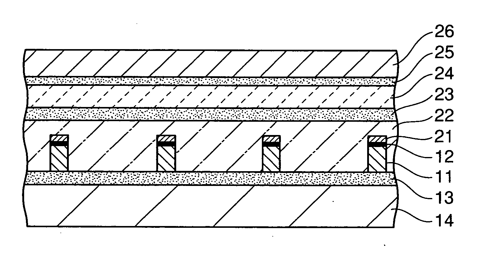
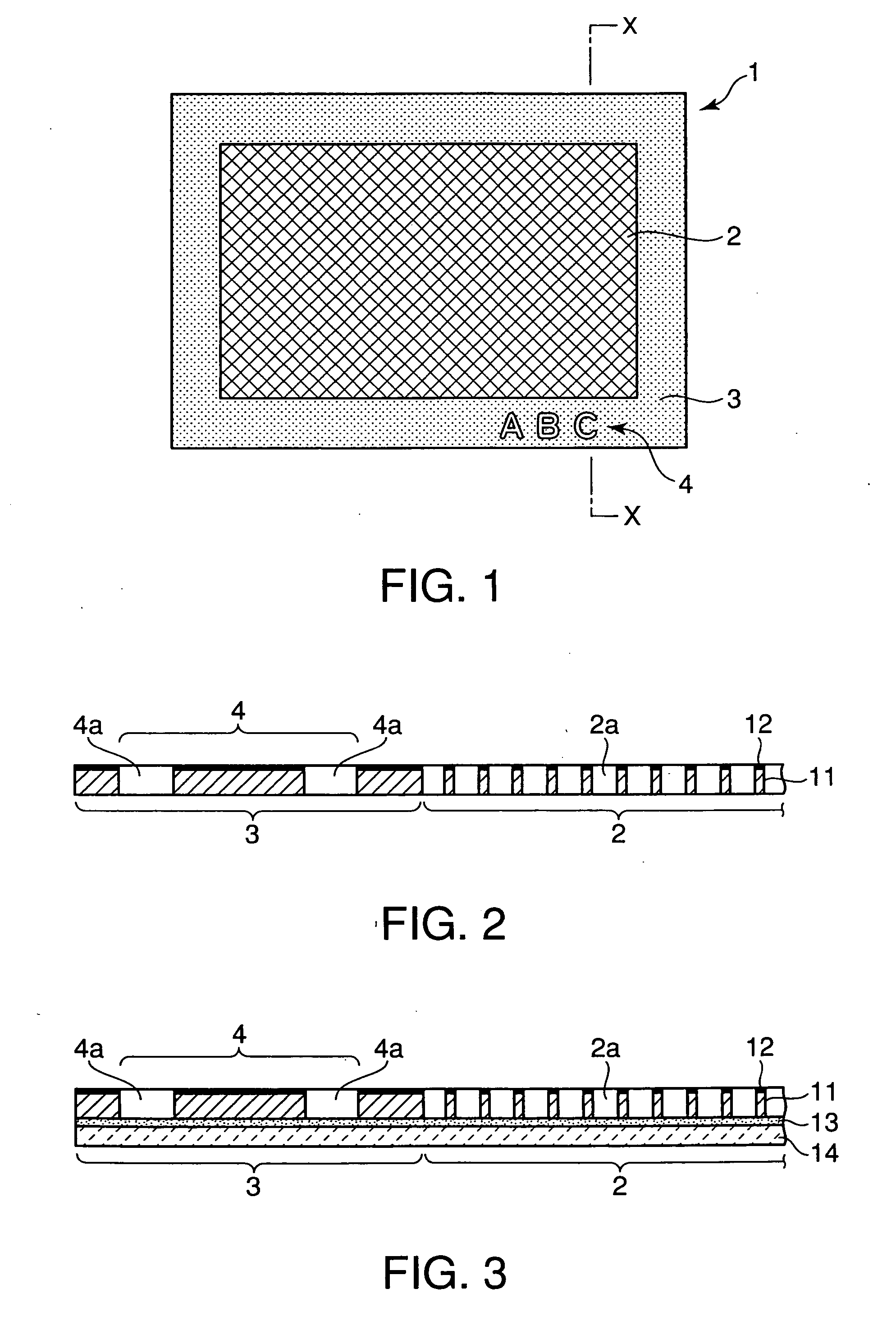
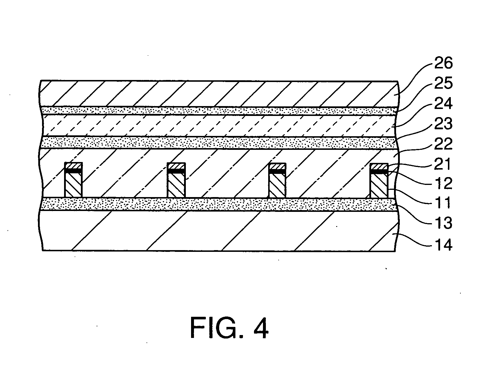
[0042]FIG. 1 is a plane view showing an electromagnetic wage shielding material according to the present invention; FIG. 2 is a sectional view showing an example of section X-X in FIG. 1; FIG. 3 is a sectional view showing another example of section X-X in FIG. 1; FIG. 4 is a sectional view showing another embodiment of the sectional structure shown in FIG. 3; FIG. 5(A) is a front view showing a display according to the present invention that is off, and FIG. 5(B), a front view showing this display that is on; and FIG. 6 is a sectional view showing an example of section X-X in FIG. 5(B). FIGS. 7 to 10 are for making a comparison with the present invention. FIG. 7 is a plane view showing a conventional electromagnetic wave shielding material; FIG. 8 is a sectional view showing section X-X in FIG. 7; FIG. 9(A) is a front view showing a display using a conven...


PUM


Abstract

An electromagnetic wave shielding material 1 comprises a light-shielding electrical conductor layer 11 having, on its observer-side external surface, a blackening layer 12. The electrical conductor layer 11 comprises a mesh portion 2 that has a large number of openings adjoining one another and faces the center portion 5b of the image-luminescent part 5a of a display device 5, and a frame portion 3 that surrounds the mesh portion 2 and faces the outer edge portion 5c of the image-luminescent part 5a of the display device 5. When trimming the screen of a display D with a black-colored light-shielding layer, since the electromagnetic wave shielding material 1 is used, it is not necessary to perform9 an additional printing step or the like, so that the total number of steps and material cost are not increased. Moreover, such electromagnetic wave shielding material does not cause non-uniformity in light-shielding properties compared with a light-shielding layer formed by printing. The frame portion 3 includes a light-transmitting pattern part 9 having patterned openings 4a.

Description

FIELD OF THE INVENTION [0001] The present invention relates to a display using a display device such as a cathode ray tube or a plasma display panel, and to an electromagnetic wave shielding material to be mounted on the observer-side surface of the display. BACKGROUND ART [0002] This type of displays using display devices emit, from their screens, not only visible rays that produce images, but also electromagnetic waves in a frequency band of megahertz to gigahertz (electromagnetic waves in this frequency band are hereinafter referred to simply as electromagnetic waves). In order to prevent electromagnetic interference (EMI) on electronic equipment that is caused by these electromagnetic waves, electromagnetic wave shielding materials having the function of bandpass filters, capable of transmitting visible rays but no electromagnetic waves, are mounted on the observer-side surfaces of the displays. [0003] Of these electromagnetic wave shielding materials, a typical one comprises an...

Claims


Application Information

Patent Timeline
IPC IPC(8): H01J1/18H01J1/00H01J19/00B32B7/02G09F9/00H05K9/00
CPCH05K9/0096H05K9/00
Inventor ARAKAWA, FUMIHIROFUJII, KAZUHITOKYODEN, YUKIHIRO
Owner DAI NIPPON PRINTING CO LTD
Why Eureka
Try Eureka