Analog-digital converter circuit

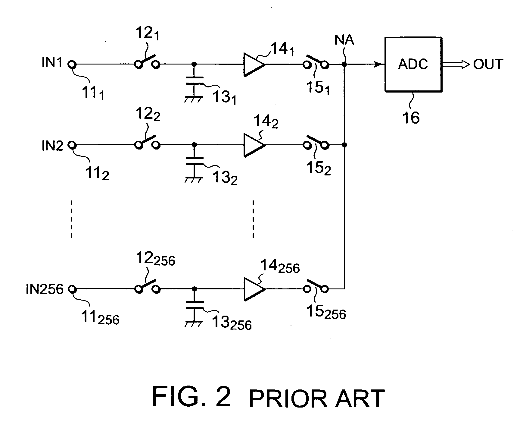
a converter circuit and analog-digital technology, applied in analogue-digital conversion, transmission systems, instruments, etc., can solve the problems of difficult to provide a large number of high-capacity buffers, drive capacity restriction, and longer response time required up to the stabilization of each voltage of the node na

Active Publication Date: 2007-08-16
LAPIS SEMICON CO LTD
View PDF5 Cites 80 Cited by
  • Summary
  • Abstract
  • Description
  • Claims
  • Application Information

AI Technical Summary

Problems solved by technology

The A / D converter circuit involves, however, the following problems.
Thus, it is difficult to provide a large number of high-capacity buffers.
Only buffers small in capacity are provided and hence drive capacity is restricted.
Therefore, a problem arises in that when each of the switches 15 is turned on and the output voltage of each buffer 14 is outputted to the node NA, a response time required up to the stabilization of each voltage of the node NA becomes longer.
This has however a fear that a layout area and current consumption increase.

Method used


Image

  • Analog-digital converter circuit
  • Analog-digital converter circuit
  • Analog-digital converter circuit

Examples


first preferred embodiment

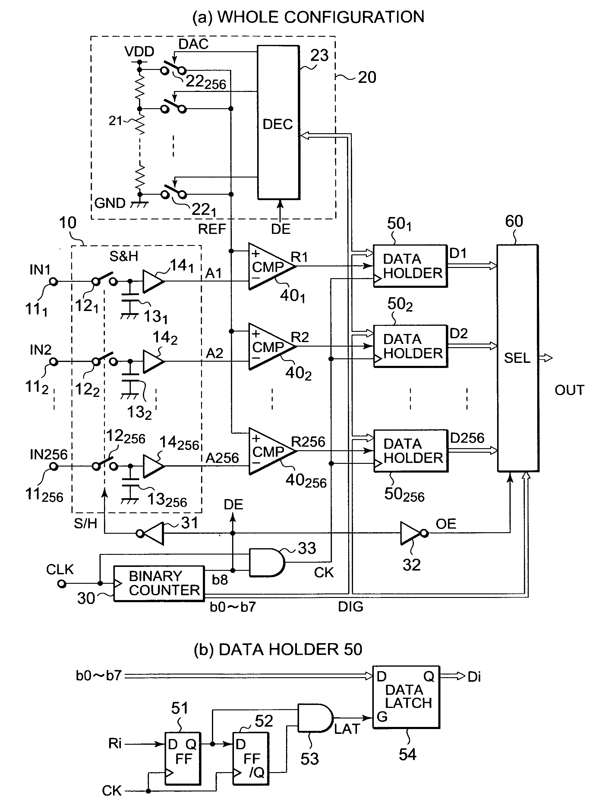
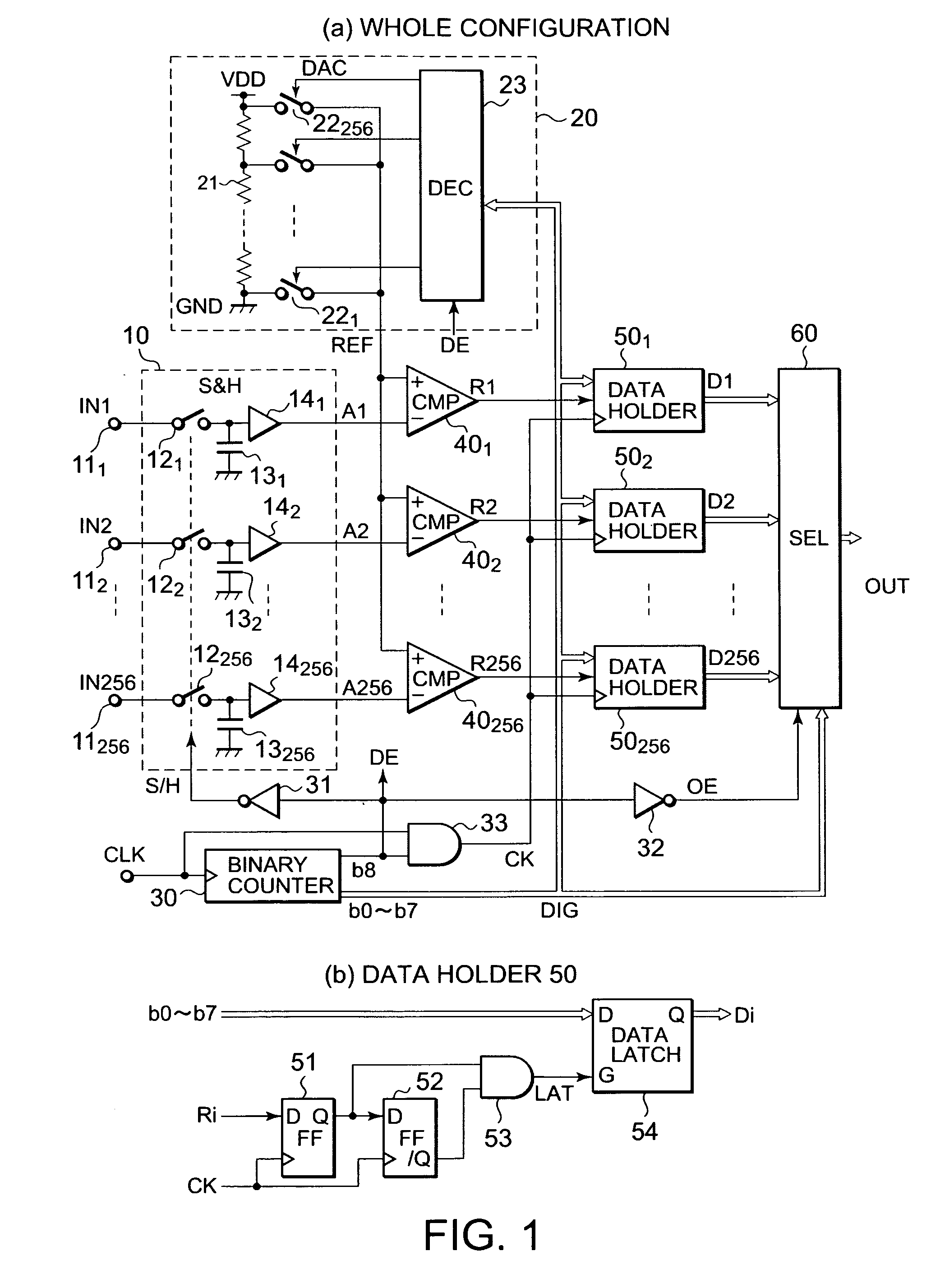
[0029]FIGS. 1(a) and 1(b) are configuration diagrams of an A / D converter circuit showing a first embodiment of the present invention.

[0030]The present A / D converter circuit processes a multi-input (e.g., 256 inputs) and includes a sample and hold unit (S&H) 10, a digital / analog converter (hereinafter called “DAC”) 20 and a binary counter 30 as shown in FIG. 1(a).

[0031]The sample and hold unit 10 has input terminals 11i respectively inputted with analog input signals INi (where i=1 to 256). Capacitors 13i and buffers 14i are respectively connected to the input terminals 11i via switches 12i. The capacitors 13i respectively hold the input signals INi sampled by the switches 12i and have other ends connected to a ground potential GND. The buffers 14i are used to output analog voltages Ai at low impedance without changing the voltages (input signals INi) retained in the capacitors 13i. The buffers 14i are constituted of voltage-follower connected operational amplifiers or the like.

[0032...

second preferred embodiment

[0052]FIG. 4 is a configuration diagram illustrative of one of comparators and one of data holders both showing a second embodiment of the present invention.

[0053]The comparator 40A and the data holder 50A are provided as an alternative to the comparators 40i and the data holders 50i shown in FIG. 1.

[0054]The comparator 40A proceeds to a low power consumption mode when a power control signal PD is given (when PD is brought to “H” in the present embodiment). The comparator can be configured by, for example, providing a switch in a power supply path of each comparator 40 shown in FIG. 1 and on / off-controlling the switch by the power control signal PD.

[0055]The data holder 50A additionally has the function of outputting a power control signal PD for the comparator 40A in addition to the function of, when a decision signal Ri changes from “L” to “H”, latching a digital value DIG and outputting the same as a digital signal Di. That is, the data holder 50A includes a set / reset type FF 55 ...

third preferred embodiment

[0059]FIG. 5 is a configuration diagram of a timing controller showing a third embodiment of the present invention.

[0060]The timing controller is provided as an alternative to the binary counter 30 and its peripheral inverters 31 and 32 and AND 33 shown in FIG. 1 in order to adapt to the arbitrary number m of input signals and the arbitrary number n of reference voltages.

[0061]The timing controller has a selector 71 for selecting and outputting a clock signal CLK during a sampling period and a hold period. A counter 72 that counts from 0 to at least m-1 during the hold period is connected to the first output side of the selector 71. A counter 73 that counts from 0 to at least n-1 during the sampling period is connected to the second output side of the selector 71.

[0062]Count values of the counters 72 and 73 are applied to their corresponding first and second input sides of a selector 74. The selector 74 selects the count value of the counter 72 during the hold period, and selects th...


PUM


Abstract

The present invention provides a multi-input A/D converter circuit capable of shorting a conversion time without increasing its layout area and current consumption. When a most significant bit of a binary counter is “L”, individual input signals are sampled by a sample and hold unit, and digital signals held in respective data holders are sequentially selected by a selector. When the most significant bit is brought to “H”, the respective input signals are held as analog signals and compared with each of reference voltages produced corresponding to a digital signal by a DAC. When decision signals outputted from comparators are changed from “L” to “H”, the digital signal at that time is held in the individual data holders as digital signals.

Description

BACKGROUND OF THE INVENTION[0001]The present invention relates to an analog / digital (hereinafter called “A / D”) converter circuit, and particularly to a multi-input A / D converter circuit.[0002]FIG. 2 is a schematic configuration diagram of a conventional A / D converter circuit.[0003]The present A / D converter circuit performs processing on a multi-input and has input terminals 11i respectively inputted with analog input signals INi (where i=1 to 256). Capacitors 13i and buffers 14i are respectively connected to the input terminals 11i via switches 12i. The capacitors 13i respectively hold the input signals INi sampled by the switches 12i and have other ends connected to a ground potential GND. The buffers 14i are used to output the voltages (input signals INi) held in the capacitors 13i at low impedance without changing the voltages. The buffers 14i are constituted of voltage-follower connected operational amplifiers or the like. A node NA is connected to the output sides of the buffer...

Claims


Application Information

Patent Timeline
Patent Type & Authority Applications(United States)
IPC IPC(8): H03M1/12
CPCH03M1/123H03M1/12H03M1/34
Inventor YAMADA, TOSHIMI
Owner LAPIS SEMICON CO LTD
Why Eureka
Try Eureka