Light emitting diode package and method of manufacturing the same
- Summary
- Abstract
- Description
- Claims
- Application Information
AI Technical Summary
Benefits of technology
Problems solved by technology
Method used
Image

Examples
first embodiment
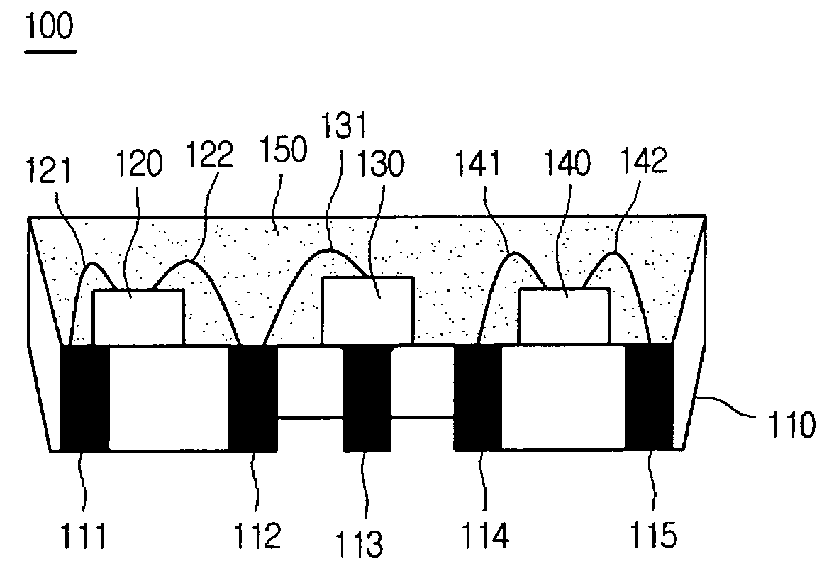
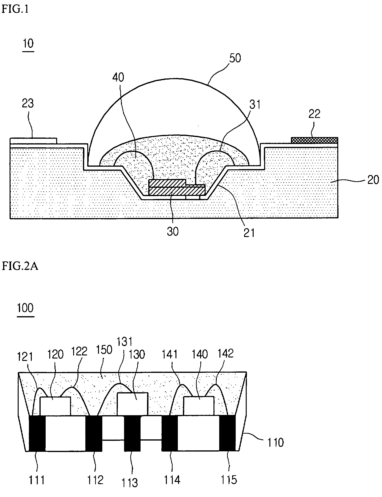
[0027]FIG. 2A is a side sectional view of an LED package according to the present invention. FIG. 2B is a circuit diagram of LEDs of FIG. 2A.
[0028]Referring to FIG. 2A, an LED package 100 includes a package main body 110 with a cavity, a plurality of lead frames 111˜115, a plurality of LED chips 120, 130 and 140, and a mold member 150 to provide light laterally.
[0029]The package main body 110 may be formed by performing injection-molding using plastic materials such as polycarbonate (PC), polycarbonate acrylonitrile butadiene styrene (PCABS), polyphthalamide (PPA), nylon, polyethylene terephtalate (PET), and polybutylene terephtalate (PBT). The lead frames 111˜115 are formed inside the cavity when molding the package main body 110. The cavity is formed to a predetermined depth at an upper portion of the package main body 110, and may have an upper diameter larger than a lower diameter. For example, each side surface of the cavity may be formed so as to lean outward at 105-120 degree...
second embodiment
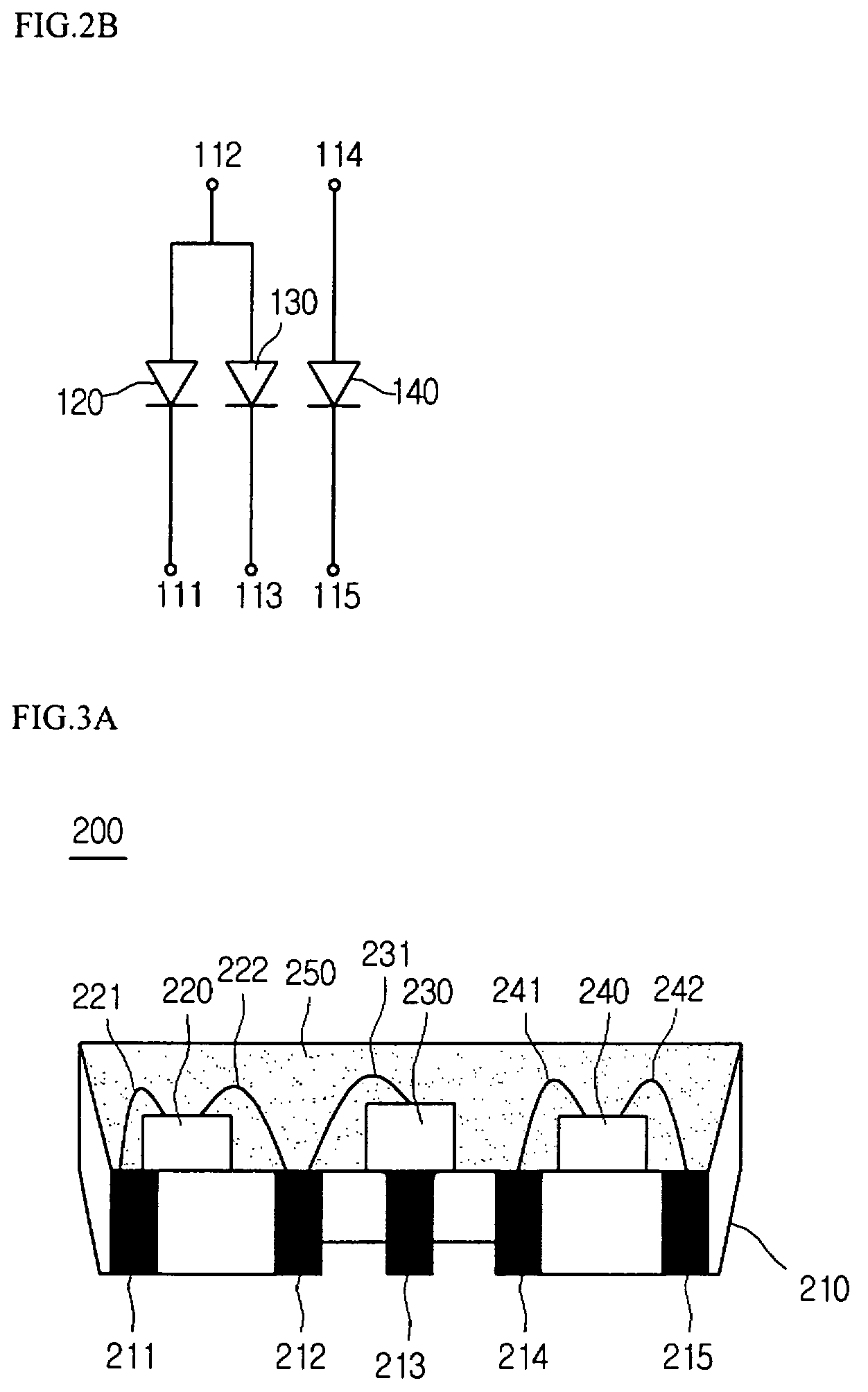
[0042]FIG. 3A is a side sectional view of an LED package according to the present invention. FIG. 3B is a circuit diagram of LEDs of FIG. 3A.
[0043]Referring to FIGS. 3A and 3B, an LED package 200 includes a package main body 210 with a cavity, a plurality of lead frames 211˜215, a plurality of LED chips 220, 230 and 240, and a mold member 250.
[0044]The package main body 210 may be formed by performing injection-molding using plastic materials such as polycarbonate (PC), polycarbonate acrylonitrile butadiene styrene (PCABS), polyphthalamide (PPA), nylon, polyethylene terephtalate (PET), and polybutylene terephtalate (PBT). The lead frames 211˜215 are formed inside the cavity when molding the package main body 210. The cavity is formed to a predetermined depth at an upper portion of the package main body 210, and may have an upper diameter larger than a lower diameter. For example, each side surface of the cavity may be formed so as to lean outward at 105-120 degree angle, thereby inc...
third embodiment
[0058]FIG. 4A is a side sectional view of an LED package according to the present invention. FIG. 4B is a circuit diagram of LEDs of FIG. 4A.
[0059]Referring to FIGS. 4A and 4B, an LED package 300 includes a package main body 310 with a cavity, a plurality of lead frames 311˜315, a plurality of LED chips 320, 330 and 340, and a mold member 350.
[0060]The package main body 310 may be formed by performing injection-molding using such as polycarbonate (PC), polycarbonate acrylonitrile butadiene styrene (PCABS), polyphthalamide (PPA), nylon, polyethylene terephtalate (PET), and polybutylene terephtalate (PBT). The lead frames 311˜315 are formed inside the cavity when molding the package main body 310. The cavity is formed to a predetermined depth at an upper portion of the package main body 310, and may have an upper diameter larger than a lower diameter. For example, each side surface of the cavity may be formed so as to lean outward at 105-120 degree angle, thereby increasing the light ...
PUM
 Abstract
Description
Claims
Application Information
 - Generate Ideas
- Intellectual Property
- Life Sciences
- Materials
- Tech Scout
- Unparalleled Data Quality
- Higher Quality Content
- 60% Fewer Hallucinations
Browse by: Latest US Patents, China's latest patents, Technical Efficacy Thesaurus, Application Domain, Technology Topic, Popular Technical Reports.
© 2025 PatSnap. All rights reserved.Legal|Privacy policy|Modern Slavery Act Transparency Statement|Sitemap|About US| Contact US: help@patsnap.com