Optical switching device

a switching device and optical switch technology, applied in the field of optical switch devices, can solve the problems of affecting the performance of error-free reception in the optical receiver, affecting the accuracy of optical switch modules, etc., to achieve the effect of reducing the error due to the wavelength dependence of optical switch modules

Inactive Publication Date: 2007-08-23
FUJITSU LTD
View PDF6 Cites 13 Cited by
  • Summary
  • Abstract
  • Description
  • Claims
  • Application Information

AI Technical Summary

Benefits of technology

[0015] The present invention has been accomplished in view of the above problems and has an object to provide an optical switching device capable of, even in the case where an optical switch module has the wavelength dependence, performing the setting and switching of optical routes by accurately grasping a characteristic relating to a loss in the optical switch module, and also of compensating for the loss in the optical switch module while suppressing the waveform degradation of an output signal light to the minimum.
[0018] According to the optical switching device of the present invention, the reference light is given to the optical switch module in the direction inverse to the propagation direction of the signal light, so that the loss in the optical switch module can be monitored using the reference light whose wavelength is set to be within the wavelength band of the input signal light. Thus, it becomes possible to acquire the loss data in which an error due to the wavelength dependence of the optical switch module is reduced. Then, the control parameter for the optical switch module is corrected based on the loss data, so that a variation in the power of the signal light output from each of the output ports can be suppressed. Further, since the reference light is supplied to each of the optical amplifiers irrespective of a generation state of the signal light, it becomes possible to perform the loss compensation of the optical switch module while suppressing a transient response of each of the optical amplifiers at the rising time of the signal light.

Problems solved by technology

However, there is caused a problem in that, when such processing is performed, there may be an influence by a difference in input power to the optical switch module, a loss difference between the input and output ports of the optical switch module or the like, so that a variation occurs in output power values of the output frame signal lights, thereby affecting the performance of error-free reception in an optical receiver.
However, even in this invention in the prior application, there remains a problem as shown in the following which is caused by the wavelength dependence of the optical switch module.
Therefore, in the case where the characteristic of the optical switch module 100 includes the wavelength dependence, there is a problem in that an error occurs in the information (calibration data) obtained by using the reference light Lb whose wavelength is different from that of the signal light Ls.
However, it is difficult to perform the error correction with sufficient precision in the case where the characteristic of the optical switch module 100 is changed due to, for example, the temperature variation, the degradation with time or the like.
Therefore, the configuration becomes complicated and also the cost thereof rises.
Further, in the device configuration shown in FIG. 6, the relatively large loss occurs in the optical switch module 100, but this loss is not compensated in the optical switching device.
Although it becomes possible to compensate for the loss as described above by disposing an optical amplifier in the optical switching device, a transient response in the optical amplifier becomes problematic only by simply disposing the optical amplifier.
To be specific, as shown in FIG. 7 for example, if the burst signal light of waveform as shown in the lower left of the figure is input to the optical amplifier disposed in the optical switching device, at the rising time of the burst signal light, a surge as shown in the lower right of the figure occurs in the output waveform of the signal light amplified by the optical amplifier, to adversely affect on the various devices connected to the downstream of the optical switching device.

Method used


Image

  • Optical switching device
  • Optical switching device
  • Optical switching device

Examples


Embodiment Construction

[0027] Hereinafter, embodiments of the present invention will be described with reference to drawings. The same reference numerals denote the same or equivalent parts in all drawings.

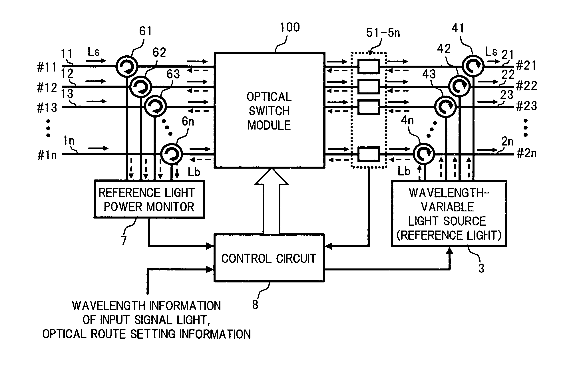
[0028]FIG. 1 is a block diagram showing a configuration of one embodiment of an optical switching device according to the present invention.

[0029] In FIG. 1, the present optical switching device comprises, for example; input ports #11 to #1n and output ports #21 to #2n; an optical switch module 100 using optical deflection elements as shown in FIG. 5; input light paths 11, 12, . . . , 1n which connect the input ports #11 to #1n to respective input ports of the optical switch module 100; and output light paths 21, 22, . . . , 2n which connect the output ports #21 to #2n to respective output ports of the optical switch module 100. Further, the present optical switching device comprises: a wavelength-variable light source 3 serving as a reference light generating section, which generates a reference ligh...


PUM


Abstract

In the present optical switching device, a reference light of a wavelength same as or in the vicinity of a wavelength of a signal light, is given from a wavelength-variable light source via each output side optical circulator to each pertinent output light path, and is propagated through each of the output light paths in a direction inverse to a propagation direction of the signal light, and passes through each optical amplifier to be sent to an optical switch module. Then, the power of the reference light which is led to each input side optical circulator from each input light path in accordance with the optical route setting by the optical switch module, is monitored by a reference light power monitor, and loss data is acquired by a control circuit using the monitoring result, so that the optical switch module is controlled in accordance with a control parameter corrected based on the loss data. Thus, it becomes possible to grasp accurately a loss characteristic of the optical switch module to perform the setting and switching of optical routes, and also, to compensate for a loss in the optical switch module while suppressing the waveform degradation of an output signal light to the minimum.

Description

BACKGROUND OF THE INVENTION [0001] 1. Field of the Invention [0002] The present invention relates to an optical switching device for performing the setting and switching of optical routes between a plurality of input and output ports, and in particular, to an optical switching device suitable for the use in constructing an optical communication system which is capable of processing a signal light containing large volume information while maintaining an optical state thereof, without converting the signal light into electrical signals. [0003] 2. Description of the Related Art [0004] In a photonic network in a metropolitan access area, a network configuration is frequently modified by the exchange of lines and signals and the switching of routes in an add / drop multiplexing (ADM) node or the like. In a repeating stage in the current network, there is often adopted a configuration in which an optical signal is once converted into an electrical signal and then is converted into an optica...

Claims


Application Information

Patent Timeline
Patent Type & Authority Applications(United States)
IPC IPC(8): H04J14/00H04B10/27H04B10/07H04B10/294
CPCG02B6/3512G02B6/3546G02B6/356G02B6/3586H04Q2011/0049G02B6/3594H04J14/0221H04Q11/0005H04Q2011/0035G02B6/359
Inventor TAKITA, YUTAKA
Owner FUJITSU LTD
Why Eureka
Try Eureka