Method For Manufacturing Electronic Components, Mother Substrate, And Electronic Component

a technology for electronic components and mother substrates, applied in the direction of stacked capacitors, fixed capacitor details, semiconductor/solid-state device details, etc., can solve the problems of difficult to improve the reliability of the coil component performance, disadvantageous and unnecessarily performing plating on the exposed portion of the dummy pattern, and generating delamination (peeling between layers). , the effect of reducing the amount of insulating material in the gap between the patterns in the layer surfa

Inactive Publication Date: 2007-08-30
MURATA MFG CO LTD
View PDF1 Cites 34 Cited by
  • Summary
  • Abstract
  • Description
  • Claims
  • Application Information

AI Technical Summary

Benefits of technology

[0016] In a method for manufacturing electronic components, according to preferred embodiments of the present invention, when insulating layers and conductive pattern layers having conductive patterns which are formed at intervals therebetween in layer surface directions are alternately laminated to form a laminate in which laminate portions of electronic component-forming conductive patterns are collectively formed, electronic component-forming conductive patterns are formed in at least one of the conductive pattern layers which are to be laminated to each other, and at positions at which the conductive patterns are not formed, removal dummy patterns and floating dummy patterns are formed. Accordingly, in accordance with the formation of the removal dummy patterns and the floating dummy patterns, the amount of the pattern formed at positions at which the electronic component-forming conductive patterns are not formed is increased. In other words, the gap between the patterns in the layer surface direction is decreased. As a result, the amount of an insulating material for the insulating layers in the gap between the patterns in the layer surface direction is decreased. Thus, the gap between the conductive patterns in the lamination direction is easily obtained substantially as designed.
[0017] In addition, in the method for manufacturing electronic components, according to preferred embodiments of the present invention, since the amount of an insulating material for the insulating layer in the gap between the patterns in the layer surface direction is decreased, the irregularities of the upper surface of the laminate formed from the conductive pattern layers and the insulating layers are reduced, and the upper surface of the laminate is planarized. Accordingly, in a step of pressing the laminate, a pressing force is approximately uniformly applied to the whole laminate, and the generation of delamination is prevented.

Problems solved by technology

Therefore, the electrical properties of the coil component 30 are varied, and as a result, it has been difficult to improve the reliability of the performance of the coil component 30.
However, when the dummy pattern 35 is formed to have a large width, the following problems may occur.
The coil component 30 separated from the laminate 33 may be processed by plating for surface treatment in some cases, and in this case, plating is disadvantageously and unnecessarily performed onto the exposed portion of the dummy pattern 35.
To prevent the problems described above, when the dummy pattern 35 is formed to have a small width, a problem may occur in that delamination (peeling between layers) is generated as described below.
Accordingly, the electrical properties of the coil component 30 are seriously degraded, and the components may be disadvantageously rejected as defective.

Method used


Image

  • Method For Manufacturing Electronic Components, Mother Substrate, And Electronic Component
  • Method For Manufacturing Electronic Components, Mother Substrate, And Electronic Component
  • Method For Manufacturing Electronic Components, Mother Substrate, And Electronic Component

Examples


Embodiment Construction

[0034] Hereinafter, preferred embodiments of the present invention will be described with reference to the figures.

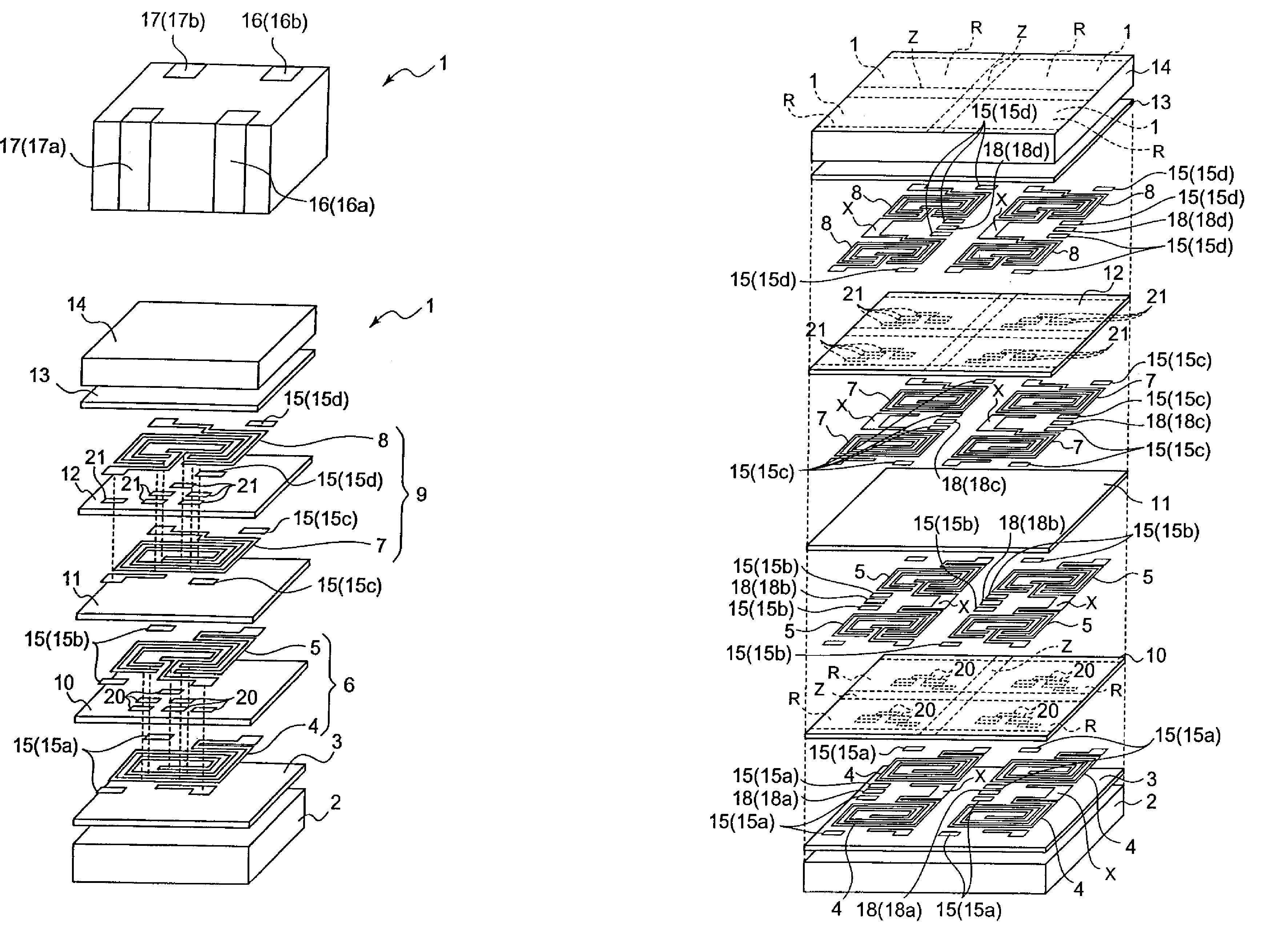
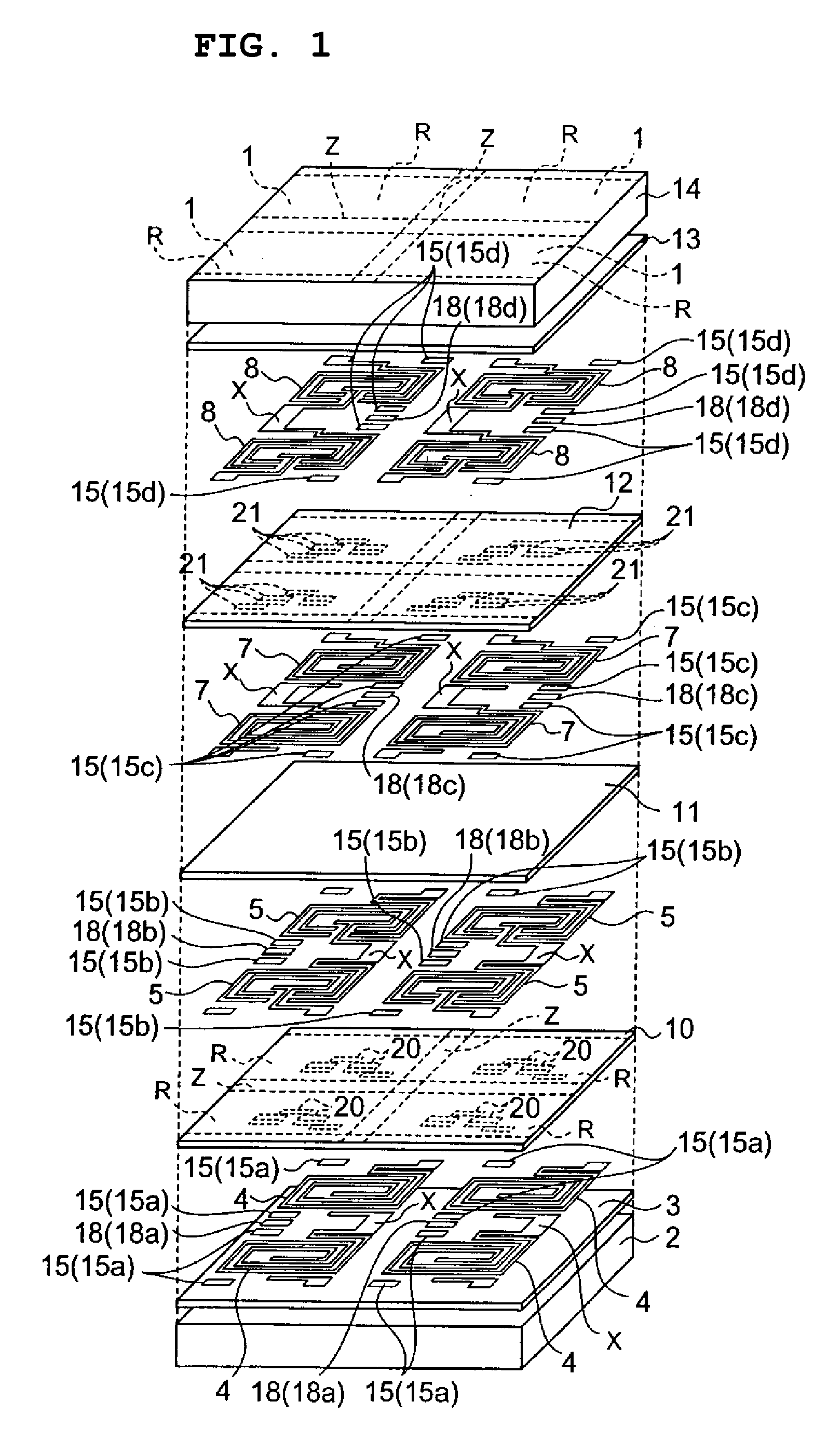
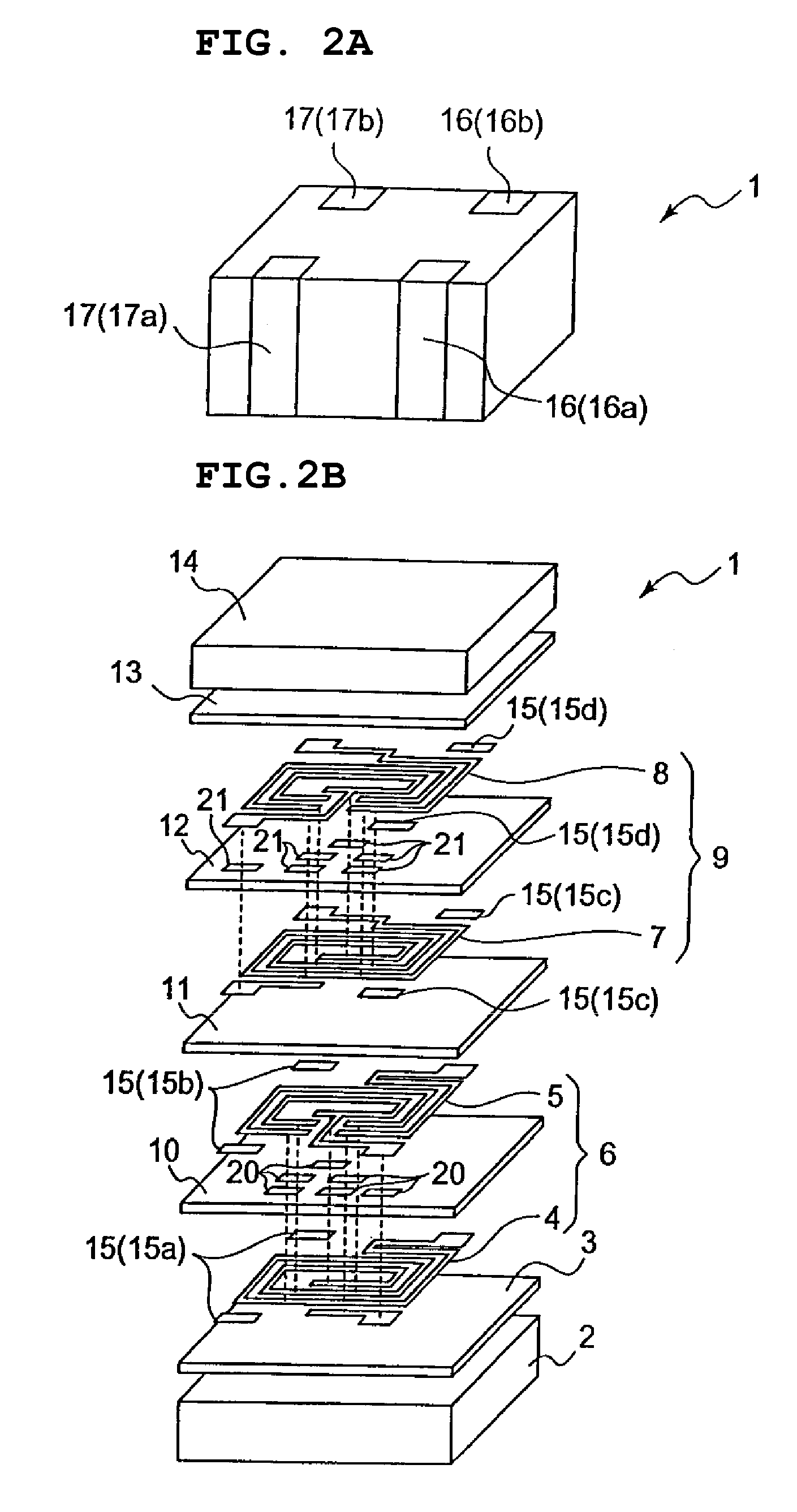
[0035] In a schematic perspective view of FIG. 2A and a schematic exploded view of FIG. 2B, a coil component (common mode choke coil component) 1, which is an electronic component of this preferred embodiment, is shown. This coil component 1 includes a base-side magnetic substrate 2, an underlying insulating layer 3, a primary coil 6 made of conductive patterns 4 and 5 which are coil patterns, a secondary coil 9 made of conductive patterns 7 and 8 which are coil patterns, conductive pattern-interlayer insulating layers 10, 11, and 12, a protective insulating layer 13, a lid-side magnetic substrate 14, floating dummy patterns 15, and exterior connection electrodes 16 (16a, 16b) and 17 (17a, 17b).

[0036] The structure of this coil component 1 will be described together with respect to a preferred embodiment of its manufacturing process. In the manufacturing process of th...


PUM

PropertyMeasurementUnit
conductiveaaaaaaaaaa
forceaaaaaaaaaa
sizeaaaaaaaaaa

Abstract

In a manufacturing process of electronic components which include conductive patterns laminated with insulating layers provided therebetween, conductive pattern layers having conductive patterns formed at intervals therebetween along layer surfaces and insulating layers are alternately laminated to each other. The laminate is pressed by applying a force thereto in the lamination direction, followed by cutting of the laminate along cutting lines provided along boundaries between the electronic components, so that the electronic components are separated from each other. In a cutting-removal region of a mother substrate from which the electronic components are separated from each other by cutting, removal dummy patterns having a size allowing it to be disposed within the above region are formed. In the electronic component, floating dummy patterns which are not electrically connected to the conductive patterns are formed at intervals from the cutting-removal region.

Description

BACKGROUND OF THE INVENTION [0001] 1. Field of the Invention [0002] The present invention relates to a method for manufacturing electronic components including conductive patterns that are laminated to each other with insulating layers provided therebetween, to a mother substrate, and to an electronic component. [0003] 2. Description of the Related Art [0004] In FIG. 5A, one example of a coil component is shown by a schematic perspective view. In FIG. 5B, a schematic cross-sectional view of the coil component in FIG. 5a taken along a line A-A is shown (for example, see Patent Document 1). This coil component 30 includes coiled conductive patterns 31 (31A and 31B) that are laminated to each other with an insulating layer 32 provided therebetween. [0005] The coil component 30 is manufactured as described below. As shown in FIG. 6A, a conductive pattern layer is formed which includes the conductive patterns 31 provided at intervals therebetween on the same plane. Conductive pattern lay...

Claims


Application Information

Patent Timeline
Patent Type & Authority Applications(United States)
IPC IPC(8): H01F27/28
CPCH01F17/0013H01F41/041H01G4/012H01G4/30H05K1/0306H05K3/0052Y10S438/96H05K3/4629H05K2201/09781Y10T29/49156Y10T29/49126Y10T29/42H05K3/4611
Inventor KUDO, KAZUHIDEMATSUNAGA, MINORU
Owner MURATA MFG CO LTD
Why Eureka
Try Eureka