Warp-free semiconductor wafer, and devices using the same

a technology of semiconductor wafers and semiconductor devices, applied in the field of semiconductor devices, can solve problems such as and achieve the effect of reducing the warpage of semiconductor wafers

Inactive Publication Date: 2007-09-13
SANKEN ELECTRIC CO LTD
View PDF1 Cites 101 Cited by
  • Summary
  • Abstract
  • Description
  • Claims
  • Application Information

AI Technical Summary

Benefits of technology

[0008]The present invention has it as an object to reduce the wa

Problems solved by technology

The result is the minimiza

Method used


Image

  • Warp-free semiconductor wafer, and devices using the same
  • Warp-free semiconductor wafer, and devices using the same
  • Warp-free semiconductor wafer, and devices using the same

Examples


embodiment

of FIG. 3

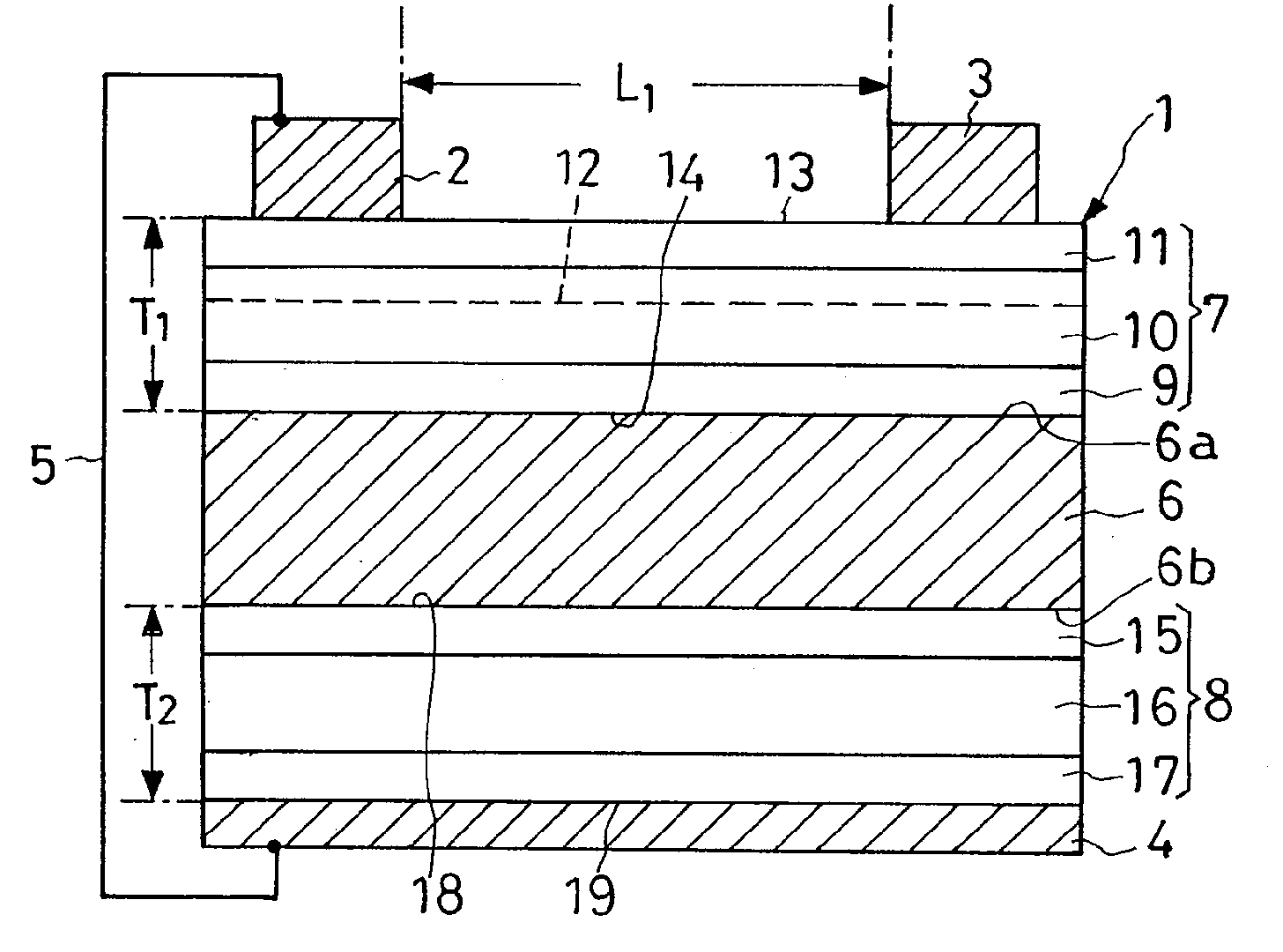
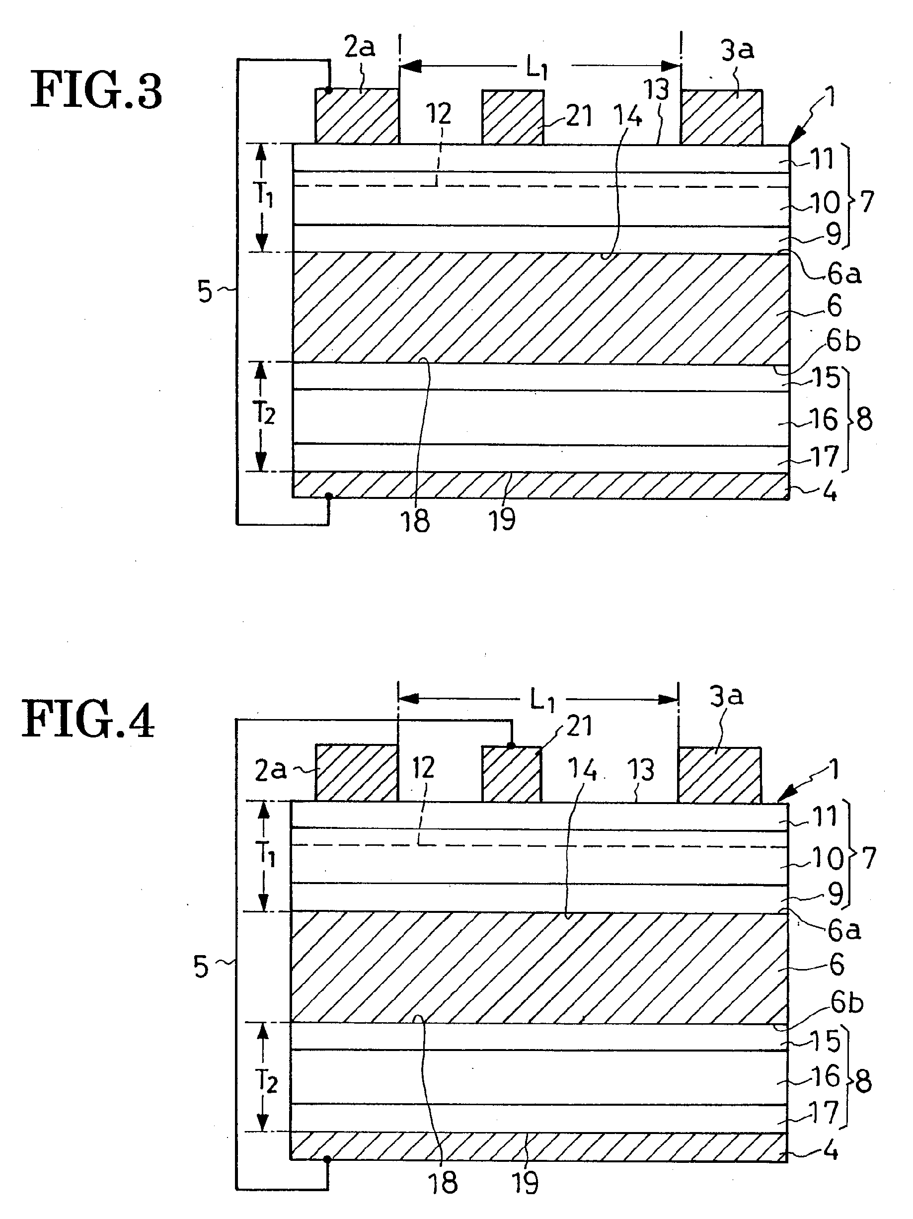
[0056]The invention is here shown applied to a HEMT. Made from the die 1 of the same design as the SBD die 1 of FIG. 1, the HEMT differs from the SBD in having a source 2a as a first main electrode and drain 3a as a second main electrode in places of the anode 2 and cathode 3 of the SBD and in additionally having a gate or gate electrode 21 between source and drain.

[0057]The source 2a and drain 3a are both in ohmic contact with the surface 13 of the main semiconductor region 7. Like the cathode 3 of the FIG. 1 embodiment, the source 2a and drain 3a may both be laminations of titanium (Ti) and aluminum (Al) layers. The gate 21 on the other hand is in Schottky contact with the main semiconductor region surface 13 and, like the anode 2 of the FIG. 1 embodiment, may be a lamination of nickel and gold layers. The back electrode 4 is coupled to the anode 2a via the conductor 5.

[0058]The HEMT die 1 being of the same construction as the SBD die 1 of FIG. 1, the two-dimensional elec...


PUM


Abstract

A semiconductor wafer to be diced into individual SBDs, HEMTs or MESFETs has a substrate with a main semiconductor region and counter semiconductor region formed on its opposite surfaces. The main semiconductor region is configured to provide the desired semiconductor devices. In order to counterbalance the warping effect of the main semiconductor region on the substrate, as well as to enhance the voltage strength of the devices made from the wafer, the counter semiconductor region is made similar in configuration to the main semiconductor region. The main semiconductor region and counter semiconductor region are arranged in bilateral symmetry as viewed in a cross-sectional plane at right angles with the substrate surfaces.

Description

CROSS REFERENCE TO RELATED APPLICATIONS[0001]This application claims priority to Japanese Patent Application No. 2006-062653, filed Mar. 8, 2006, the disclosure of which is incorporated herein by reference in its entirety.BACKGROUND OF THE INVENTION[0002]This invention relates to semiconductors in general and, in particular, to a semiconductor wafer and to semiconductor devices utilizing the same. The invention specifically pertains to field-effect transistors (FETs), Schottky-barrier diodes (SBDs), and high-electron-mobility transistors (HEMTs), among other semiconductor devices.[0003]The metal-semiconductor FET (MESFET) and HEMT have been both known and used extensively which are made from semiconducting nitrides on silicon substrates. Japanese Unexamined Patent Publication No. 2005-158889 is hereby cited as dealing with these kinds of semiconductor devices. One of the problems with such semiconductor devices arose when they were put to use in a “floating” state, that is, with the...

Claims


Application Information

Patent Timeline
IPC IPC(8): H01L29/74
CPCH01L29/2003H01L29/7787H01L29/42316H01L29/205H01L29/872
Inventor GOTO, HIROKAZU
Owner SANKEN ELECTRIC CO LTD
Why Eureka
Try Eureka