Vertical-type surrounding gate semiconductor device

a semiconductor device and vertical-type technology, applied in the field of semiconductor devices, can solve the problems of saving manufacturing costs

Inactive Publication Date: 2007-09-13
PROMOS TECH INC
View PDF4 Cites 18 Cited by
  • Summary
  • Abstract
  • Description
  • Claims
  • Application Information

AI Technical Summary

Benefits of technology

[0010] Accordingly, the object of the present invention is to provide a vertical-type surrounding gate semiconductor device capable of inhibiting the floating body effect, thereby avoiding various derived problems.

Problems solved by technology

On the other hand, the ground line is formed in the pillar substrate without occupying the usable area of the device, so the manufacturing cost is saved.

Method used


Image

  • Vertical-type surrounding gate semiconductor device
  • Vertical-type surrounding gate semiconductor device
  • Vertical-type surrounding gate semiconductor device

Examples


Embodiment Construction

[0021] Reference will now be made in detail to the present preferred embodiments of the invention, examples of which are illustrated in the accompanying drawings. Wherever possible, the same reference numbers are used in the drawings and the description to refer to the same or like parts.

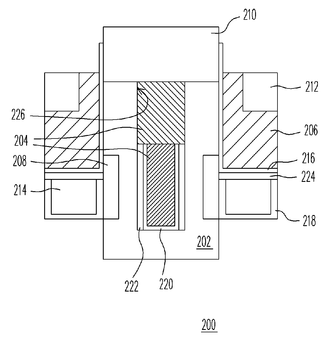
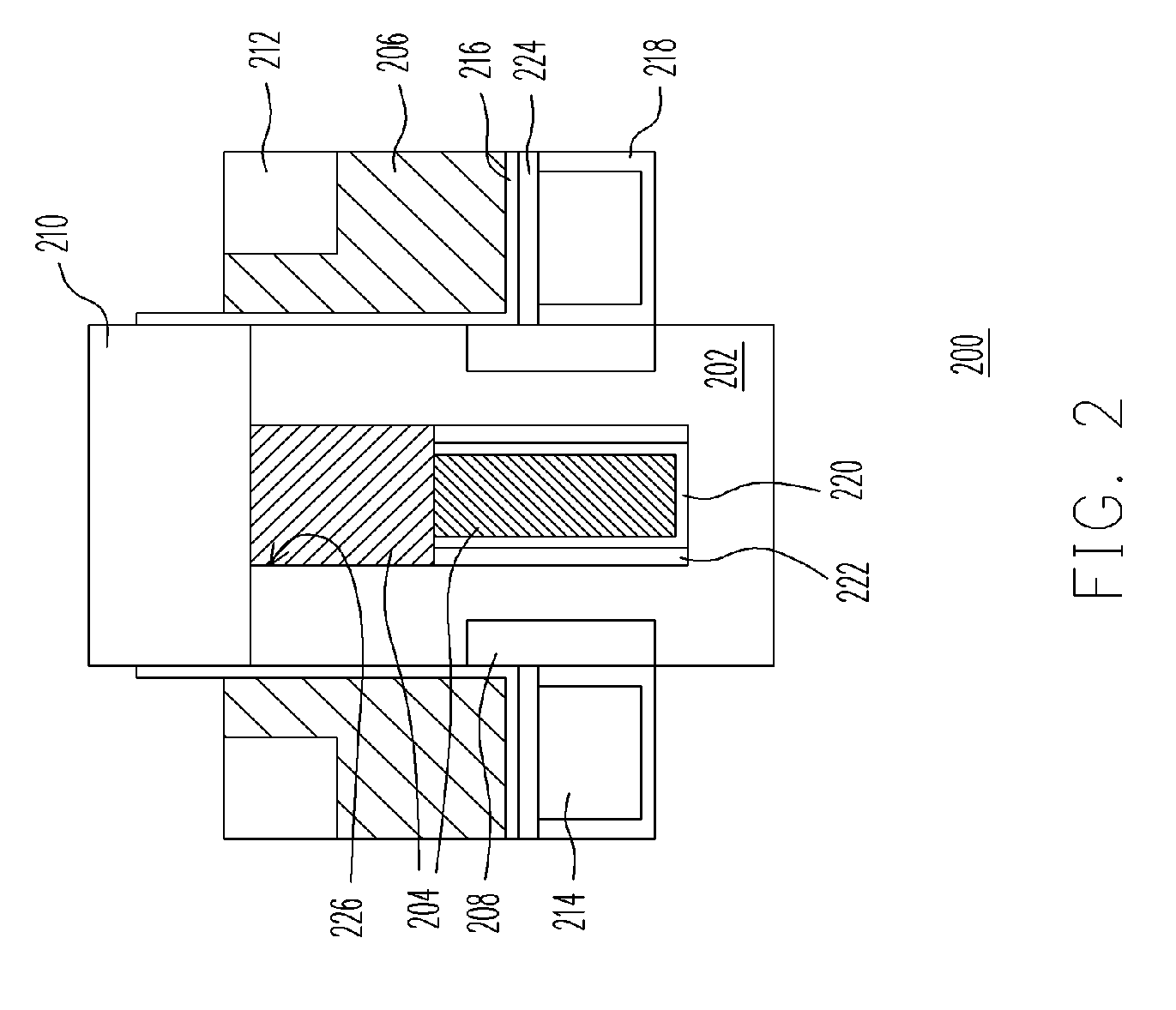
[0022]FIG. 2 is a schematic sectional view of the vertical-type surrounding gate semiconductor device according to one embodiment of the present invention.

[0023] Referring to FIG. 2, the vertical-type surrounding gate semiconductor device 200 comprises a pillar substrate 202, a ground line 204, a gate 206, a source region 208, a drain region 210, a word line 212, a bit line 214, a gate dielectric layer 216, metal layers 218 and 220, a collar oxide layer 222 and a dielectric layer 224.

[0024] The pillar substrate 202 has an opening 226. The collar oxide layer 222 is disposed on the sidewall of the lower portion of the opening 226. The metal layer 220 is disposed on the bottom of the opening 226 and...


PUM


Abstract

A vertical-type surrounding gate semiconductor device is described. The semiconductor device comprises a pillar substrate, a collar oxide layer, a metal layer, a drain region, a ground line, a source region, a bit line, a word line, a gate and a gate dielectric layer. The ground line is formed in an opening of the pillar substrate and electrically connected to the pillar substrate, and covers the collar oxide layer and the metal layer. The drain region is formed on the top of the pillar substrate and in the upper portion of the opening. The gate is formed among the word line, the bit line and the pillar substrate. The gate dielectric layer is formed among the gate, the source region, the drain region, the bit line and the pillar substrate.

Description

CROSS-REFERENCE TO RELATED APPLICATION [0001] This application claims the priority benefit of Taiwan application serial no. 95108075, filed on Mar. 10, 2006. All disclosure of the Taiwan application is incorporated herein by reference. BACKGROUND OF THE INVENTION [0002] 1. Field of Invention [0003] The present invention relates to a semiconductor device. More particularly, the present invention relates to a semiconductor device with a vertical-type surrounding gate. [0004] 2. Description of Related Art [0005] With the miniaturization of devices, in order to satisfy different applications of the integrated circuit industry in future, at present, the transistor configuration of semiconductor devices is progressing from a planar gate to a vertical gate. [0006]FIG. 1A is a schematic stereogram of a transistor of a conventional vertical-type gate semiconductor device. FIG. 1B is a schematic sectional view of FIG. 1A along the section line I-I′. [0007] Referring to FIGS. 1A and 1B, the ve...

Claims


Application Information

Patent Timeline
Patent Type & Authority Applications(United States)
IPC IPC(8): H01L31/00
CPCH01L29/456H01L29/517H01L29/7827H01L29/66666H01L29/518
Inventor WU, HSIAO-CHE
Owner PROMOS TECH INC
Why Eureka
Try Eureka