

Display
a technology of optical display and particle moving type, applied in the field of display, can solve the problems of deterioration of optical characteristics, increase in cost, deterioration of electrical characteristics, etc., and achieve the effects of high reflectivity, high contrast ratio, and high quality display
- Summary
- Abstract
- Description
- Claims
- Application Information
AI Technical Summary
Benefits of technology
Problems solved by technology
Method used
Image

Examples
embodiment 1
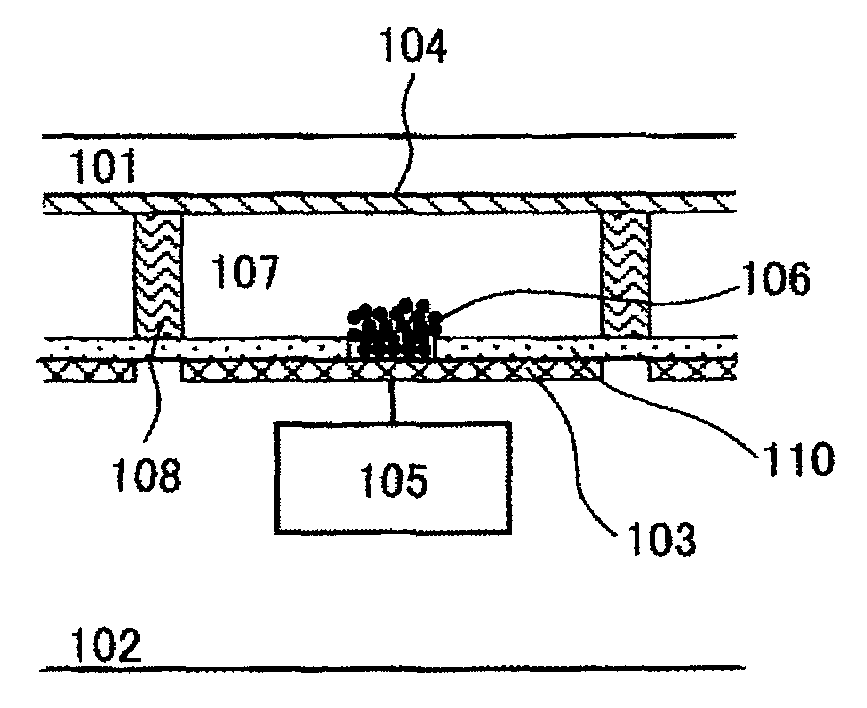
[0097]Next, one embodiment of the display according to the present invention will be described more specifically along with a manufacturing method therefor with reference to FIGS. 1A and 1B and FIG. 11.
[0098]FIG. 1A and 1B are cross-sectional diagrams of the display. A particle driving means 105, as a switching part, is formed on a glass substrate 102 in a two-dimensional array. On the glass substrate 102, a pixel electrode 103 is deposited by sputtering thereon using a metal material having a high reflectivity such as Al. Thereafter, the pixel electrode 103 is pattern-processed in a square shape through photolithography and wet etching. Furthermore, after an insulating layer 110 comprised of SiO2 is deposited thereon through a plasma CVD method, openings are processed by lithography and dry etching. Moreover, partitions that each comprises cardo polymer and has a height of 5 μm are patterned into a lattice state to form the partitions 108. The part between the partitions 108 is fil...
embodiment 2
[0104]Next, another embodiment of the present display will be described more specifically along with a manufacturing method therefor with reference to FIGS. 8A and 8B.
[0105]A cross-sectional structure of a display of the present embodiment is illustrated in FIG. 8B. After a pixel electrode 103 is deposited on a glass substrate 102, which is formed with particle driving means 105 that are disposed in a two dimensional array, by sputtering using a metal material having a high reflectivity such as Al, the pixel electrode 103 is patterned in a square shape through photolithography and wet etching. On the pixel electrode 103, an insulative color filter layer 112B which includes blue colorants dispersed in insulative resin and transmits only a blue wavelength region, an insulative color filter layer 112G which includes green colorants dispersed in the insulative resin and transmits only a green wavelength region, an insulative color filter layer 112R which includes dispersed red colorants...
embodiment 3
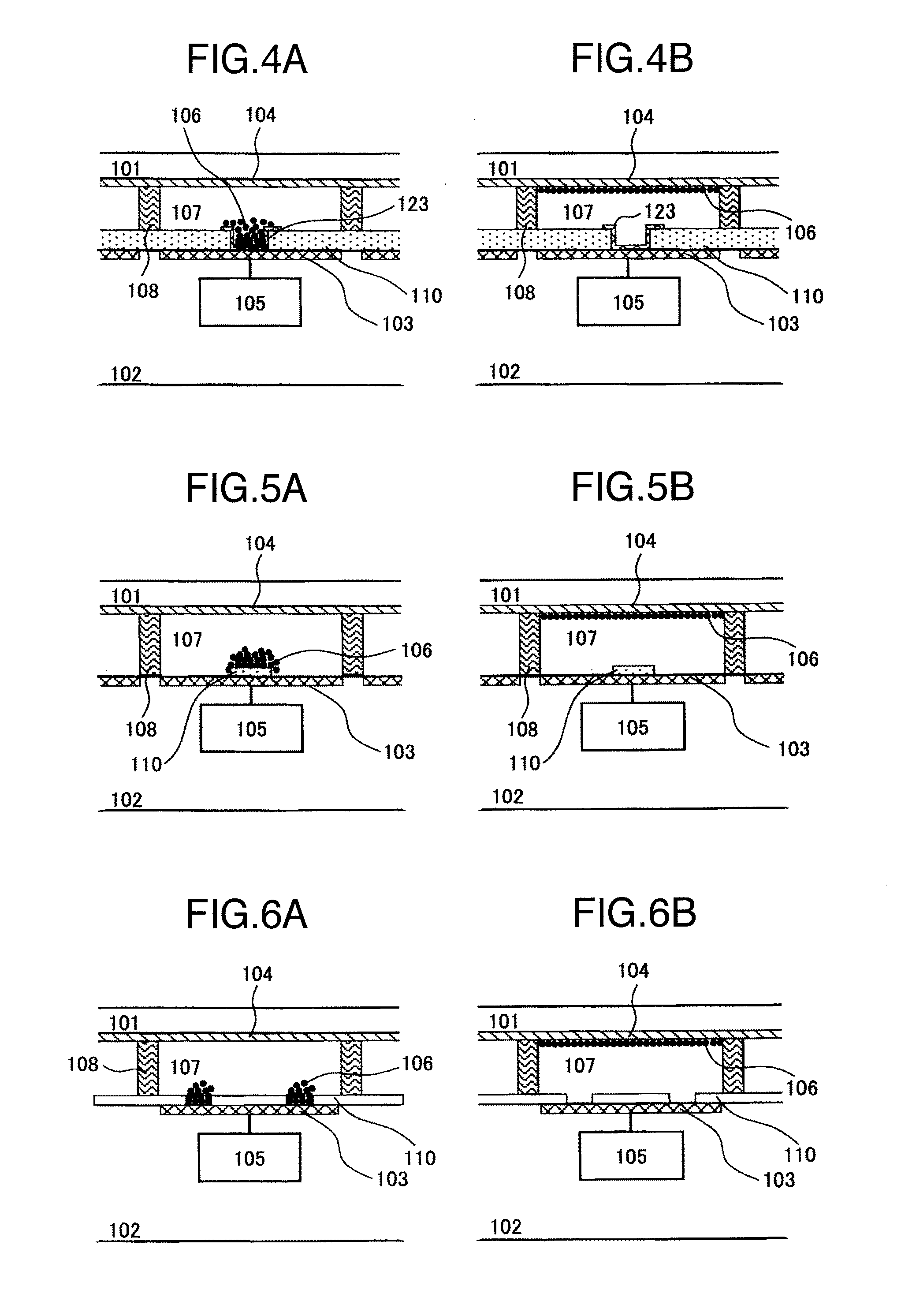
[0108]Next, another embodiment of the present display will be described more specifically with reference to FIGS. 6A, 6B, and 16.
[0109]Cross-sectional diagrams of the display of the present embodiment are illustrated in FIGS. 6A and 6B. A flexible substrate, which is coated with an insulating smoothing film made of resin, is formed on a metal thin plate, which is made of an FeNi42 alloy and has a thickness of 0.2 mm. On the flexible substrate, a particle driving means 105 is formed in a two-dimensional array as with the embodiment of FIGS. 1A, and then a pixel electrode 103, an insulating layer 110, and partitions 108 are formed. The part between the partitions 108 is filled with a transparent medium 107 that contains black charged particles 106 dispersed therein, and then sealed together with the flexible resin substrate having a thickness of 0.1 mm. Thus the display is provided.
[0110]The display according to the present invention has a plurality of openings as illustrated in FIG. ...
PUM
 Abstract
Description
Claims
Application Information