System for adjusting manufacturing equipment, method for adjusting manufacturing equipment, and method for manufacturing semiconductor device

Inactive Publication Date: 2007-09-13
KK TOSHIBA
View PDF8 Cites 9 Cited by
  • Summary
  • Abstract
  • Description
  • Claims
  • Application Information

AI Technical Summary

Benefits of technology

[0006] An aspect of present invention inheres in a system for adjusting a manufacturing equipment, according to an embodiment of the present invention. The system includes a measurement equipment configured to measure a plurality of sizes of portions of a product on a plane, an approximation module configured to approximate a planar distribution of the plurality of sizes by an orthogonal polynomial as a function of coordinates on the plane, an association module configured to associate a plurality of terms in the orthogonal polynomial with a plurality of equipment parameters of the manufacturing equipment, respectively, the manufacturing equipment manufacturing the product, and an adjusting module configured to adjust the plurality of equipment parameters to reduce a plurality of distribution components. The plurality of distribution components compose the planar distribution approximated by the orthogonal polynomial.
[0007] Another aspect of the present invention inheres in a method for adjusting the manufacturing equipment, according to the embodiment of the present invention. The method includes measuring a plurality of sizes of portions of a product on a plane, approximating a planar distribution of the plurality of sizes by an orthogonal polynomial as a function of coordinates on the plane, associating a plurality

Problems solved by technology

As the result, the yield rate of the semiconductor dev

Method used


Image

  • System for adjusting manufacturing equipment, method for adjusting manufacturing equipment, and method for manufacturing semiconductor device
  • System for adjusting manufacturing equipment, method for adjusting manufacturing equipment, and method for manufacturing semiconductor device
  • System for adjusting manufacturing equipment, method for adjusting manufacturing equipment, and method for manufacturing semiconductor device

Examples


first embodiment

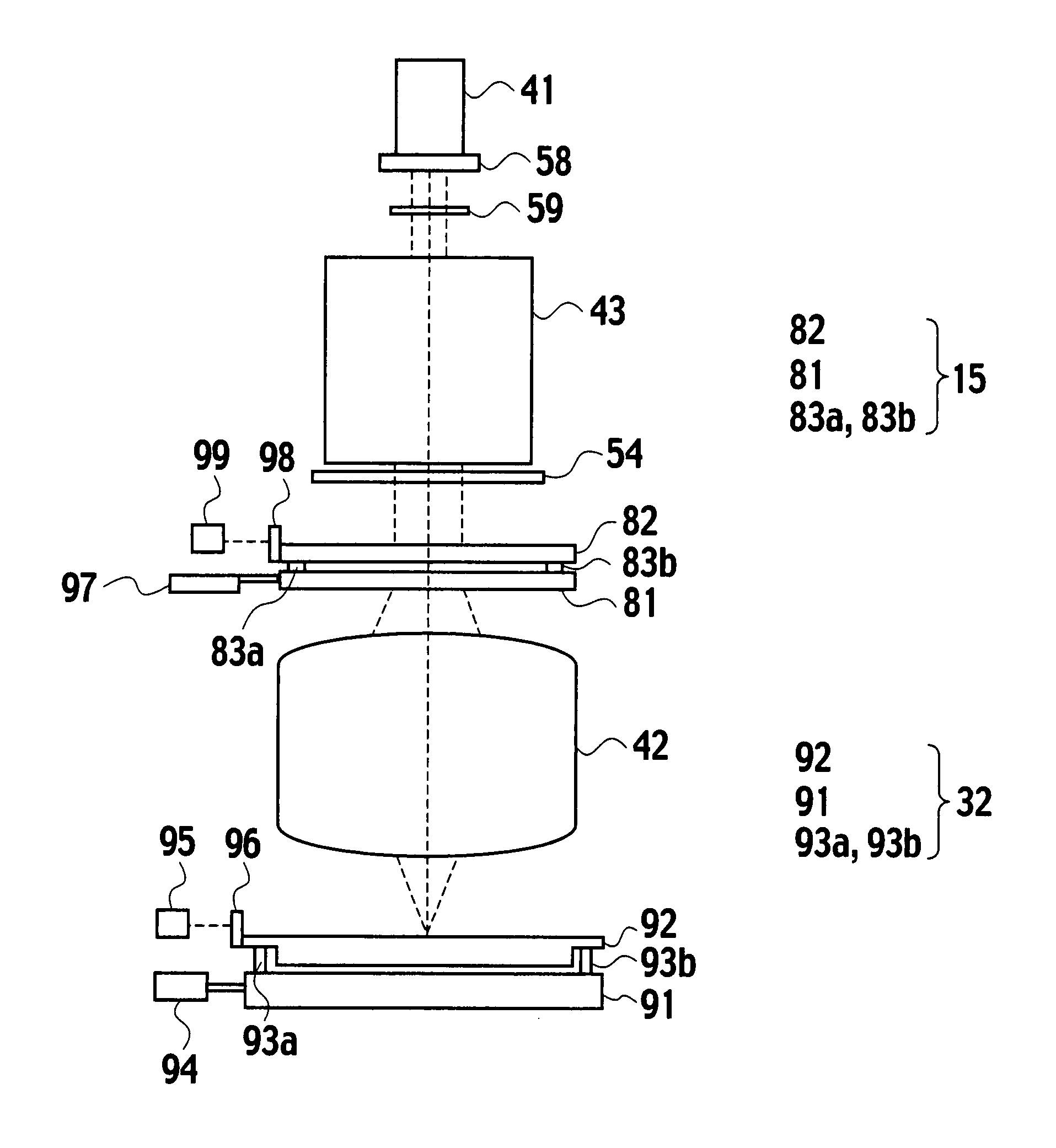
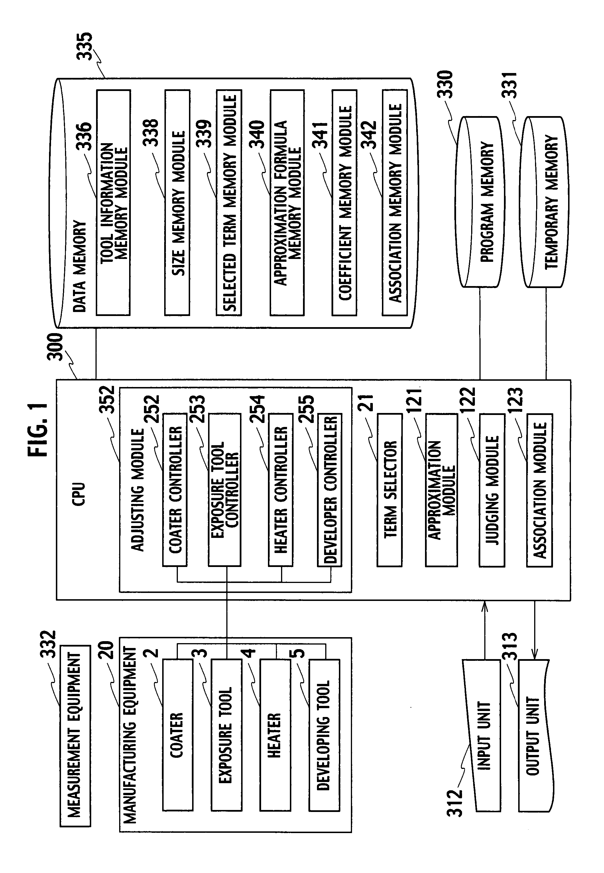
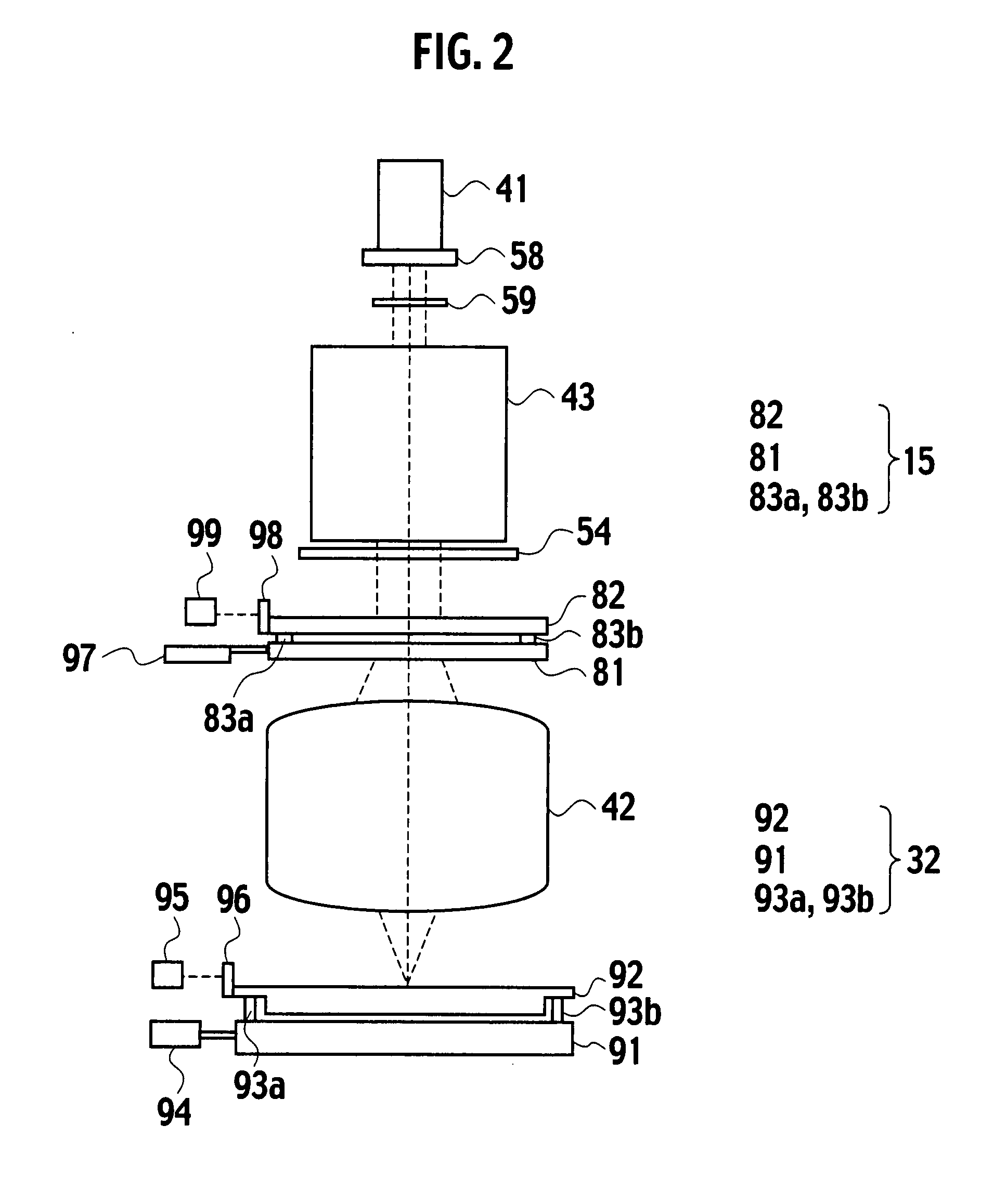
[0023] With reference to FIG. 1, a system for adjusting a manufacturing equipment, according to the first embodiment, includes a measurement equipment 332 configured to measure each size of a plurality of portions of a product on a plane and a central processing unit (CPU) 300. Here, “each size of portions of the product” means each depth of a plurality of trenches provided on a wafer such as a semiconductor substrate, each thickness of portions of a resist layer, an insulating layer, and a conductive layer on the semiconductor substrate, and each line width of portions of a resist pattern formed on the semiconductor substrate, for example. In the first embodiment, each line width of the portions of the resist pattern formed on the semiconductor substrate is took up as each size of the portions of the product.

[0024] The CPU 300 of the system for adjusting the manufacturing equipment is connected to a manufacturing equipment 20 configured to manufacture the product on the plane. The...

second embodiment

[0082] With reference to FIG. 12, the manufacturing equipment 20 connected to the CPU 300, according to the second embodiment, further includes a vapor deposition tool 1 and an etch tool 6. The vapor deposition tool 1 is configured to deposit the insulating layer on the wafer. The equipment parameters of the vapor deposition tool 1 include concentration of deposition materials, deposition time, deposition temperature, a shape of a deposition material blast nozzle, and a positional relationship between the blast nozzle and the wafer, for example. A chemical vapor deposition (CVD) tool can be used for the vapor deposition tool 1, for example.

[0083] The etch tool 6 is configured to selectively remove the insulating layer by using the resist pattern formed on the insulating layer by the coater 2, the exposure tool 3, the heater 4, and the developing tool 5 as an etchant mask. The equipment parameters of the etch tool 6 include concentration of etchant gas, etching time, etching tempera...


PUM


Abstract

A system for adjusting a manufacturing equipment includes a measurement equipment configured to measure a plurality of sizes of portions of a product on a plane, an approximation module configured to approximate a planar distribution of the plurality of sizes by an orthogonal polynomial. as a function of coordinates on the plane, an association module configured to associate a plurality of terms in the orthogonal polynomial with a plurality of equipment parameters of the manufacturing equipment, respectively, the manufacturing equipment manufacturing the product, and an adjusting module configured to adjust the plurality of equipment parameters to reduce a plurality of distribution components, the plurality of distribution components composing the planar distribution approximated by the orthogonal polynomial.

Description

CROSS REFERENCE TO RELATED APPLICATIONS AND INCORPORATION BY REFERENCE [0001] This application is based upon and claims the benefit of priority from prior Japanese Patent Application P2006-045923 filed on Feb. 22, 2006; the entire contents of which are incorporated by reference herein. BACKGROUND OF THE INVENTION [0002] 1. Field of the Invention [0003] The present invention relates to production engineering and in particular to a system for adjusting a manufacturing equipment, a method for adjusting the manufacturing equipment, and a method for manufacturing a semiconductor device. [0004] 2. Description of the Related Art [0005] As described in Japanese Patent Laid-Open Publication No. 2004-179663, when a semiconductor device is manufactured, sizes of a circuit pattern formed on a silicon wafer may vary, depending on various factors. Especially, when a large silicon wafer, such as 300 mm wafer, is used, the sizes of the circuit pattern formed on the silicon wafer tend to vary. As th...

Claims


Application Information

Patent Timeline
IPC IPC(8): H01L21/66G06F19/00H01L21/027
CPCG03F7/16G03F7/30G03F7/70616G03F7/70525G03F7/70566G03F7/705
Inventor KANNO, MASAHIROASANO, MASAFUMI
Owner KK TOSHIBA
Why Eureka
Try Eureka