

Epoxy resin composition for semiconductor encapsulation and semiconductor device using the same
Inactive Publication Date: 2007-09-13
CHEIL IND INC
View PDF3 Cites 4 Cited by
- Summary
- Abstract
- Description
- Claims
- Application Information
AI Technical Summary
Benefits of technology
[0011]It is therefore a feature of the present invention to provide an epoxy resin composition for semiconductor encapsulation that exhibits high reactivity and good storage stability.
[0012]It is another feature of the present invention to provide an epoxy resin composition for semiconductor encapsulation that exhibits improved moldability and excellent curing properties for semiconductor encapsulation.
Problems solved by technology
However, such curing of B-stage epoxy resin molding material may result in poor moldability due to a difference in thermal hysteresis between the surface and the inside of the epoxy resin material at relatively low temperatures.
In particular, use of such epoxy resin molding materials in semiconductor molding may trigger outer defects, e.g., incomplete filling, voids, pinholes, and so forth, and internal defects, e.g., deformation of gold lines, internal voids, and so forth, and, thereby, reduce semiconductor reliability, e.g., decrease moisture resistance reliability and minimized soldering heat resistance.
Reduced reactivity may cause incomplete curing reactions when conventional curing accelerators are used, thereby triggering deterioration of semiconductor moldability, curing properties and storage stability.
Method used
View moreImage
Smart ImageViewing Examples


Examples
examples 1-6
[0038]Sample epoxy resin compositions 1-6 according to an embodiment of the present invention were prepared in accordance with Table 1 below. The respective components were homogenously mixed using a Henshel mixer, melt-kneaded at 100-120° C. using a continuous kneader, cooled, and pulverized to prepare epoxy resin compositions for semiconductor molding.
examples 7-10
[0045]Sample epoxy resin compositions 7-10 according to an embodiment of the present invention were prepared in accordance with Table 3 below. The method of preparation was identical to the method used in Examples 1-6.
Login to View More PUM
| Property | Measurement | Unit |
|---|---|---|
| Fraction | aaaaa | aaaaa |
| Fraction | aaaaa | aaaaa |
| Fraction | aaaaa | aaaaa |
Abstract
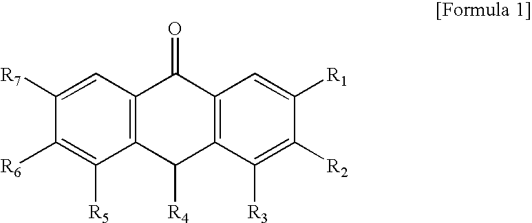
An epoxy resin composition for semiconductor encapsulation includes at least one epoxy resin, at least one curing agent, at least one filler, and at least one first curing accelerator, the first curing accelerator having a tetracyanoethylene, a 7,7,8,8-tetracyanoquinodimethane, a compound having the chemical structure of Formula 1, or a mixture thereof,wherein each of R1 through R7, independently, represents a hydrogen atom or a C1-C12 hydrocarbon group, provided that when R1 through R7 are C1-C12 hydrocarbon groups, R1 and R2, R2 and R3, R3 and R4, R4 and R5, R5 and R6, and R6 and R7 can be joined to each other to form a cyclic structure.
Description
BACKGROUND OF THE INVENTION[0001]1. Field of the Invention[0002]The present invention relates to an epoxy resin composition for semiconductor encapsulation. In particular, the present invention relates to an epoxy resin composition for semiconductor encapsulation exhibiting good flowability and excellent curing properties.[0003]2. Description of the Related Art[0004]Recent developments in high-density and automatic technology for mounting semiconductor packages on printed boards have induced surface mounting techniques, where semiconductor packages may be directly soldered onto a surface of a printed board instead of being attached thereto by lead pins. Such mounting techniques have triggered the use of flat plastic packages (FPPs) suitable for high-density and surface mounting instead of conventional dual inline packages (DIPs). The flat plastic packages may have an increased size and number of pins due to improved microprocessing technology, i.e., improved integration of semicondu...
Claims
Login to View More Application Information
Patent Timeline
 IPC IPC(8): C08L63/00
CPCC08G59/245H01L23/293C08G59/68C08G59/621H01L2924/0002Y10T428/31511H01L2924/00
InventorLEE, EUN JUNGPARK, YOON KOKLEE, YOUNG KYUNKIM, WHAN GUNCHANG, SUK KU
OwnerCHEIL IND INC