Data collector control system with automatic communication port switch
- Summary
- Abstract
- Description
- Claims
- Application Information
AI Technical Summary
Benefits of technology
Problems solved by technology
Method used
Image
Examples
case 1
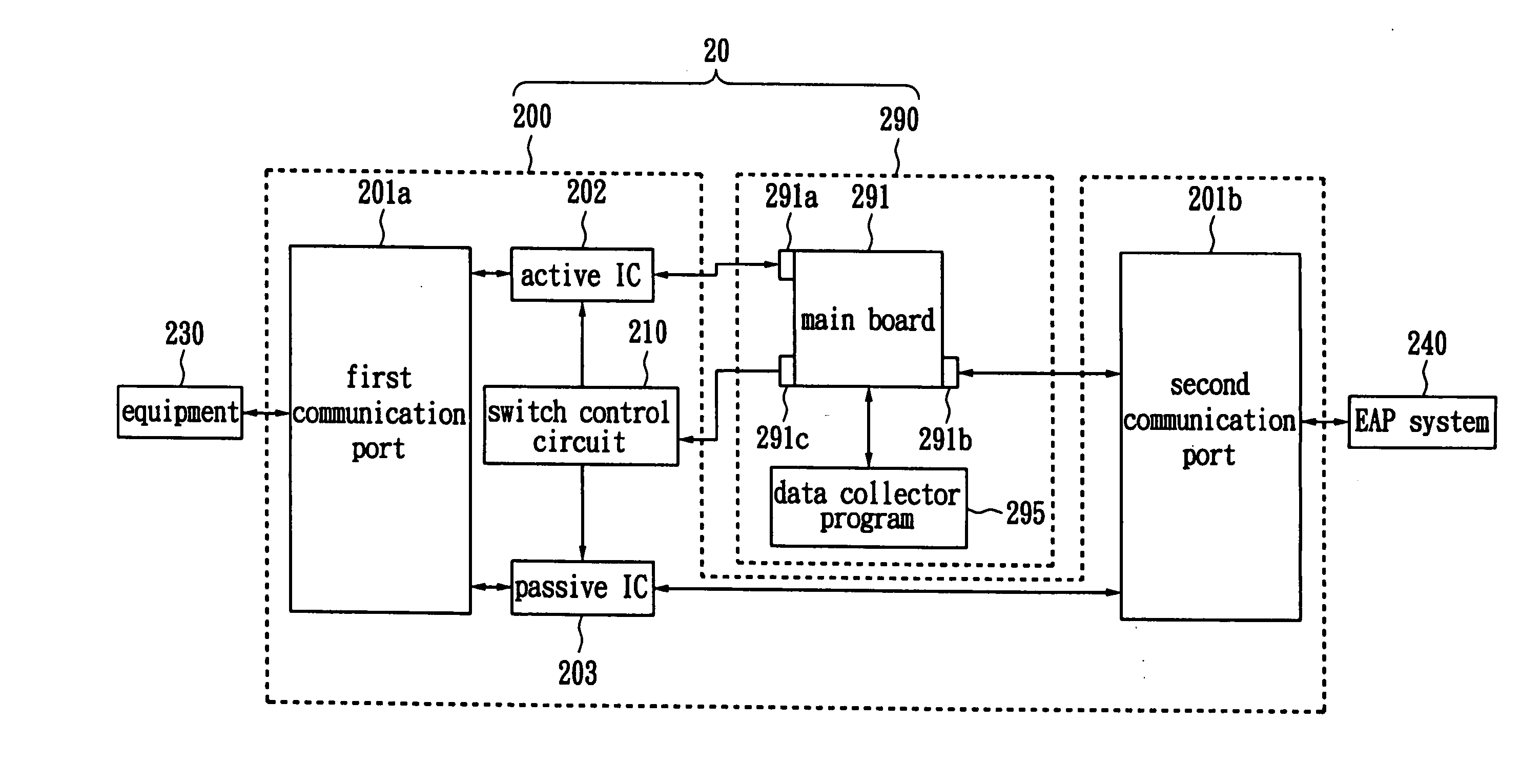
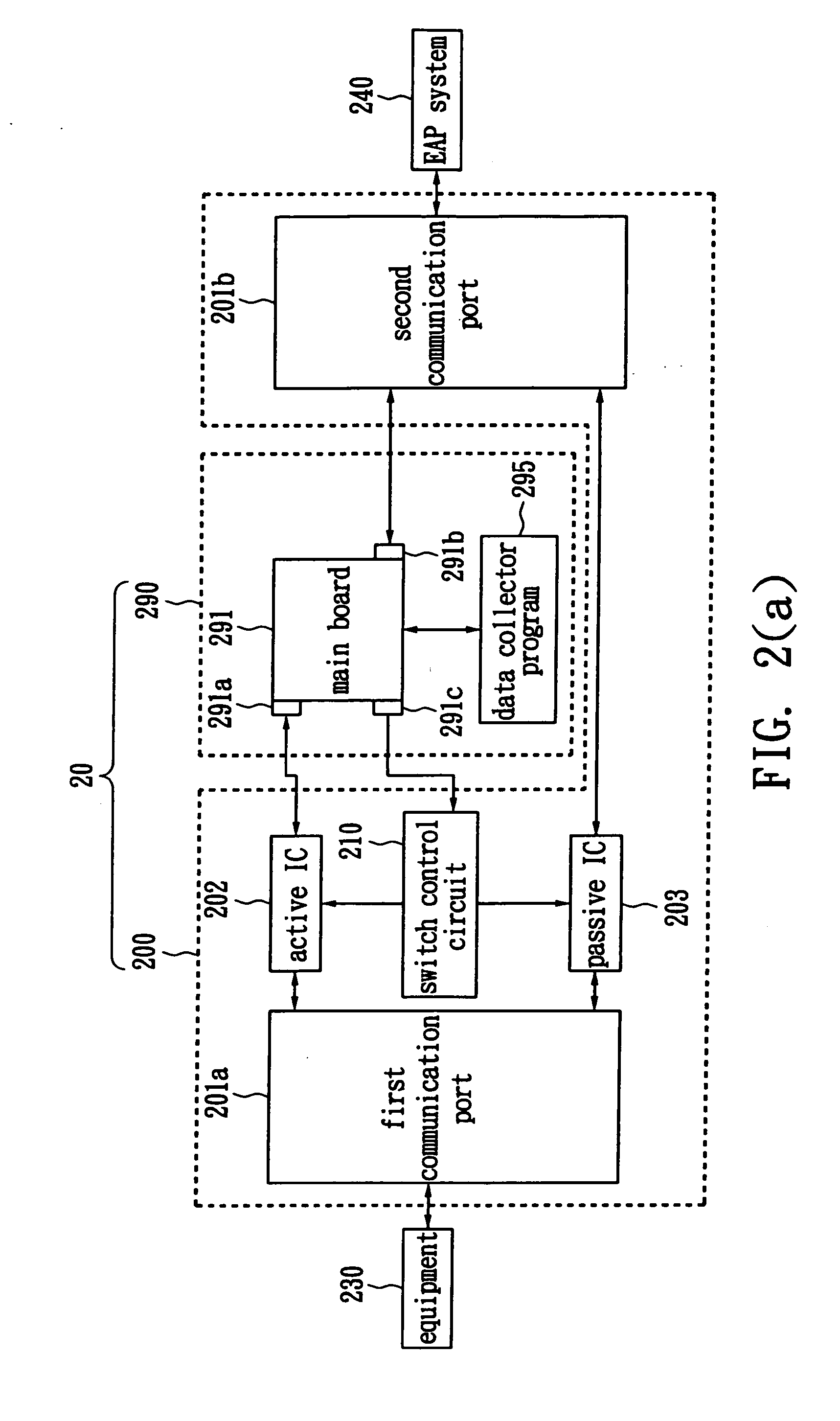
[0028] In the beginning, the data collector program 295 has not yet started, the status switch 208 is in the abnormal position, the abnormal LED indicator 207 is on and the normal LED indicator 206 is off. After starting and running the data collector program 295 for a period of time, the status switch 208 is switched to the normal position and the normal LED indicator 206 turns on. Simultaneously, the input voltage of the input point 2 of the second relay 213 drops from 5V to 0V, the common point 1 of the second relay 213 is connected to the normal close point 4 such that the input voltage of the input point 2 of the first relay 214 rises from 0V to 10V. Subsequently, the common point 1 of the first relay 214 is connected from the normal close point 4 to the normal open point 5, the abnormal LED indicator 207 turns off and the active IC 202 starts operating.
case 2
[0029] In the beginning, the data collector program 295 has not yet started, the status switch 208 is in the normal position, the common point 1 of the second relay 213 is connected to the normal close point 4, and the abnormal LED indicator 207 and the normal LED indicator 206 are on. After starting and running the data collector program 295 for a period of time, a 10V signal is generated by the delay circuit 212. As the common point 1 of the second relay 213 is connected to the normal close point 4, the input voltage of the input point 2 of the first relay 214 rises from 0V to 10V. Subsequently, the common point 1 of the first relay 214 is connected from the normal close point 4 to the normal open point 5, the abnormal LED indicator 207 turns off and the active IC 202 starts operating.
case 3
[0030] In the beginning, the data collector 290 operates normally, the status switch 208 is in the normal position, the common point 1 of the second relay 213 is connected to the normal close point 4, the abnormal LED indicator 207 is off and the normal LED indicator 206 is on. After the operating system (OS) of the main board 291 or the data collector program 295 crashes, or the hardware of the data collector system 20 is out of order, the output signal of the delay circuit 212 drops from 10V to 0V for a period of time and the input voltage of the input point 2 of the first relay 214 drops from 10V to 0V. Subsequently, the common point 1 of the first relay 214 is connected from the normal open point 5 to the normal close point 4, the abnormal LED indicator 207 turns on and the passive IC 202 starts operating.
PUM
 Abstract
Description
Claims
Application Information


