

Semiconductor device
a technology of semiconductor devices and devices, applied in semiconductor devices, semiconductor/solid-state device details, electrical apparatus, etc., can solve the problems of complex structure and manufacturing conditions, reduce the degree of flexibility of interconnection design, and not realistic, and achieve the effect of inhibiting complication
- Summary
- Abstract
- Description
- Claims
- Application Information
AI Technical Summary
Benefits of technology
Problems solved by technology
Method used
Image

Examples
first embodiment
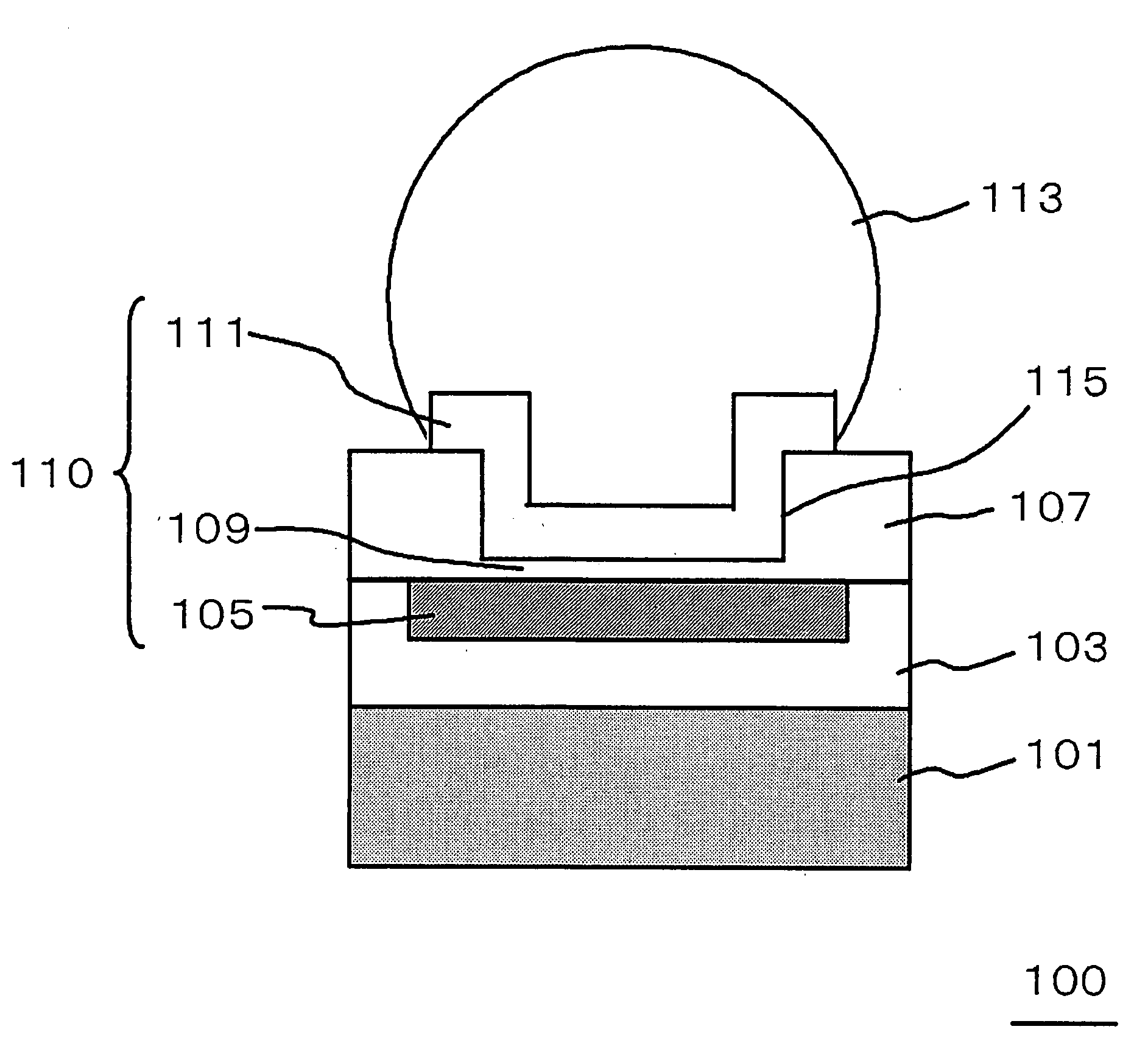
[0052]FIG. 1 is a cross-sectional view, illustrating a configuration of a semiconductor device of the present embodiment.
[0053]A semiconductor device 100 shown in FIG. 1 includes: a semiconductor substrate (silicon substrate 101); an insulating interlayer (interlayer film 103) provided on the silicon substrate 101; a multiple-layered interconnect embedded in the interlayer film 103; a electrode pad (flip-chip pad 111), provided so as to be opposite to an upper surface of an uppermost layer interconnect 105 in the multiple-layered interconnect and having a bump electrode (solder ball 113) for an external coupling mounted thereon; and a capacitance insulating film (capacitance film 109) provided between the uppermost layer interconnect 105 and the flip-chip pad 111. In the semiconductor device 100, the solder ball 113 is joined to the flip-chip pad 111.
[0054]The semiconductor device 100 includes a capacitor element 110, which is composed of the uppermost layer interconnect 105, the ca...
second embodiment
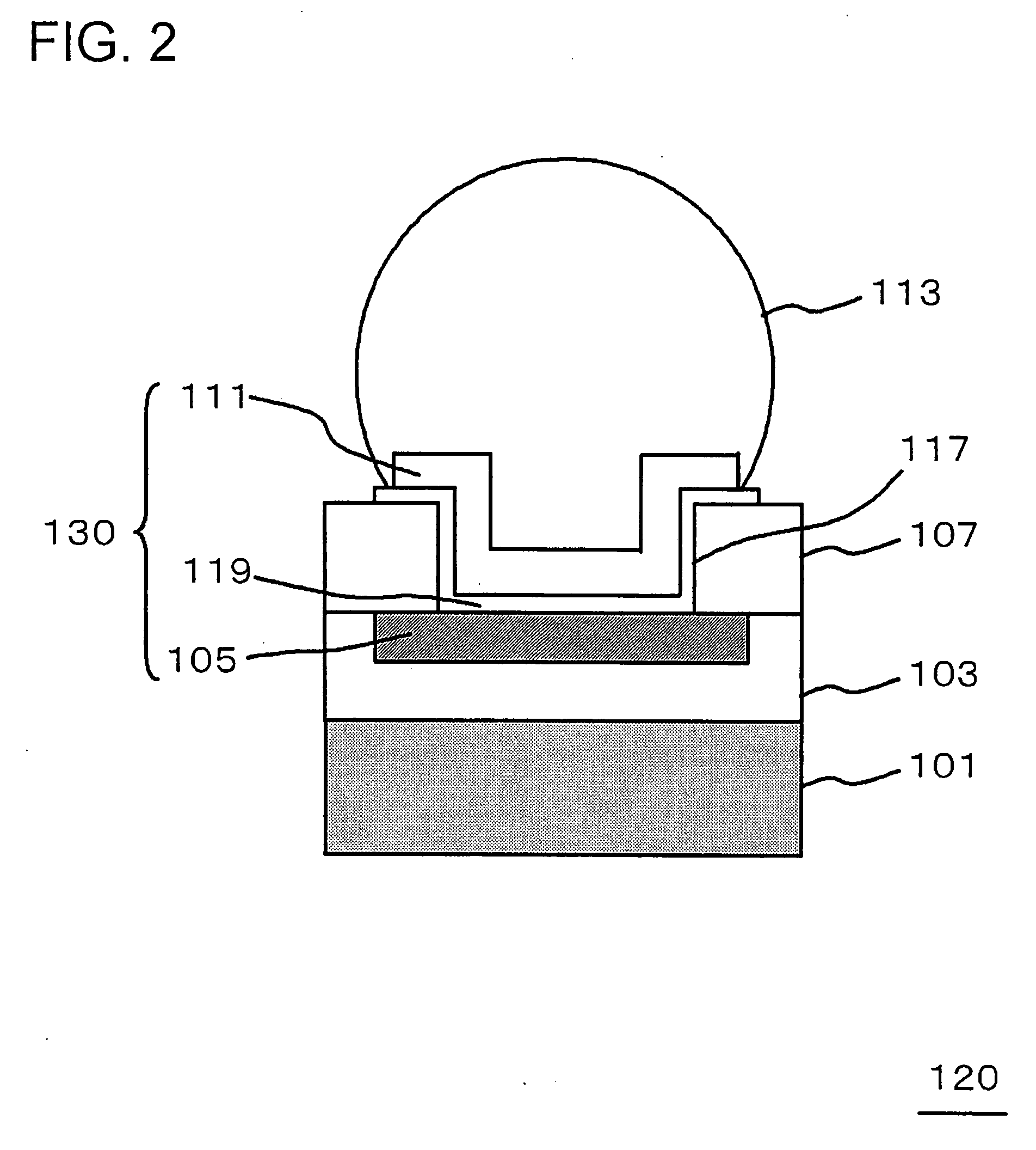
[0085]FIG. 2 is a cross-sectional view, illustrating a configuration of a semiconductor device of the present embodiment.
[0086]Fundamental configuration of a semiconductor device 120 shown in FIG. 2 is similar to that of the semiconductor device 100 described in first embodiment (FIG. 1), except that different insulating films are employed for the cover film 107 and the capacitive film 119 of the capacitor element 130, respectively.
[0087]Further, the concave portion formed in the cover film 107 corresponds to a through hole (pad via 117) that extends through the cover film 107 in the semiconductor device 120. The semiconductor device 120 includes a second insulating film (capacitive film 119) covering an interior wall of such through hole, and the flip-chip pad 111 is provided on the capacitive film 119.
[0088]The pad via 117 is a via hole provided in cover film 107 in a region where capacitor element 130 is to be formed.
[0089]In the present embodiment, the cover film 107 may be comp...
third embodiment
[0102]The configurations of the above-mentioned embodiment may alternatively be configured that the uppermost layer interconnect and the electrode pad, which constitute a capacitor element, are respectively coupled to different power supply potentials.
[0103]For example, when the uppermost layer interconnect 105 under the flip-chip pad 111 is a power supply interconnect (VDD) or a grounding interconnect (GND), the following procedure is conducted. When the uppermost layer interconnect 105 is a power supply interconnect, a pad 123 in the side of the substrate, which is coupled with the flip-chip pad 111 that constitutes the capacitance, is assigned to be for a ground, and when the uppermost layer interconnect 105 is a grounding interconnect, the pad 123 in the side of the substrate is assigned to be for a power supply. As described above, the uppermost layer interconnect 105 and the pad 123 in the side of the substrate, which is coupled with the flip-chip pad 111 that faces the upperm...
PUM
 Abstract
Description
Claims
Application Information