Method for enhancing growth of semipolar (A1,In,Ga,B)N via metalorganic chemical vapor deposition

a metalorganic chemical vapor and growth enhancement technology, applied in the direction of crystal growth process, polycrystalline material growth, chemically reactive gas, etc., can solve the undesirable quantum-confined stark effect of conventional c-plane quantum well structure in iii-nitride based optoelectronic and electronic devices, reducing carrier recombination efficiency, red-shifted emission, etc., to reduce the number of crystallographic defects

Active Publication Date: 2007-09-20
RGT UNIV OF CALIFORNIA
View PDF20 Cites 6 Cited by
  • Summary
  • Abstract
  • Description
  • Claims
  • Application Information

AI Technical Summary

Benefits of technology

[0033] The semipolar nitride semiconductor thin film has a surface morphology needed for state-of-the-art nitride semipolar electronic devices, comprising a planar film surface, fewer surface undulations, and a reduced number of crystallographic defects present in the film compared to film grown without the (Al,In,Ga)N nucleation or buffer layer.

Problems solved by technology

However, conventional c-plane quantum well structures in III-nitride based optoelectronic and electronic devices suffer from the undesirable quantum-confined Stark effect (QCSE), due to the existence of strong piezoelectric and spontaneous polarizations.
The strong built-in electric fields along the c-direction cause spatial separation of electrons and holes that in turn yield lowered carrier recombination efficiency, reduced oscillator strength, and red-shifted emission.
Unfortunately, despite advances made by researchers at the University of California, the assignee of the present invention, growth of nonpolar nitrides remains challenging and has not yet been widely adopted in the III-nitride industry.
Bulk crystals of GaN are not readily available, so it is not possible to simply cut a crystal to present a surface for subsequent device regrowth.
ELO is a cumbersome processing and growth method used to reduce defects in GaN and other semiconductors.
If the growth is stopped before the stripes coalesce, then a small area of semipolar plane, typically 10 μm wide at best, can be exposed, but this available surface area is too small to process into a semipolar LED.
Furthermore, the semipolar plane will be not parallel to the substrate surface, and forming device structures on inclined facets is significantly more difficult than forming those structures on normal continuous planes.
While the advantages of using nucleation layers (NLs) in heteroepitaxy of GaN thin films is well established, the mechanisms for how the NLs improve crystal quality are not well understood.

Method used


Image

  • Method for enhancing growth of semipolar (A1,In,Ga,B)N via metalorganic chemical vapor deposition
  • Method for enhancing growth of semipolar (A1,In,Ga,B)N via metalorganic chemical vapor deposition
  • Method for enhancing growth of semipolar (A1,In,Ga,B)N via metalorganic chemical vapor deposition

Examples


Embodiment Construction

[0040] In the following description of the preferred embodiment, reference is made to the accompanying drawings which form a part hereof, and in which is shown by way of illustration a specific embodiment in which the invention may be practiced. It is to be understood that other embodiments may be utilized and structural changes may be made without departing from the scope of the present invention.

Overview

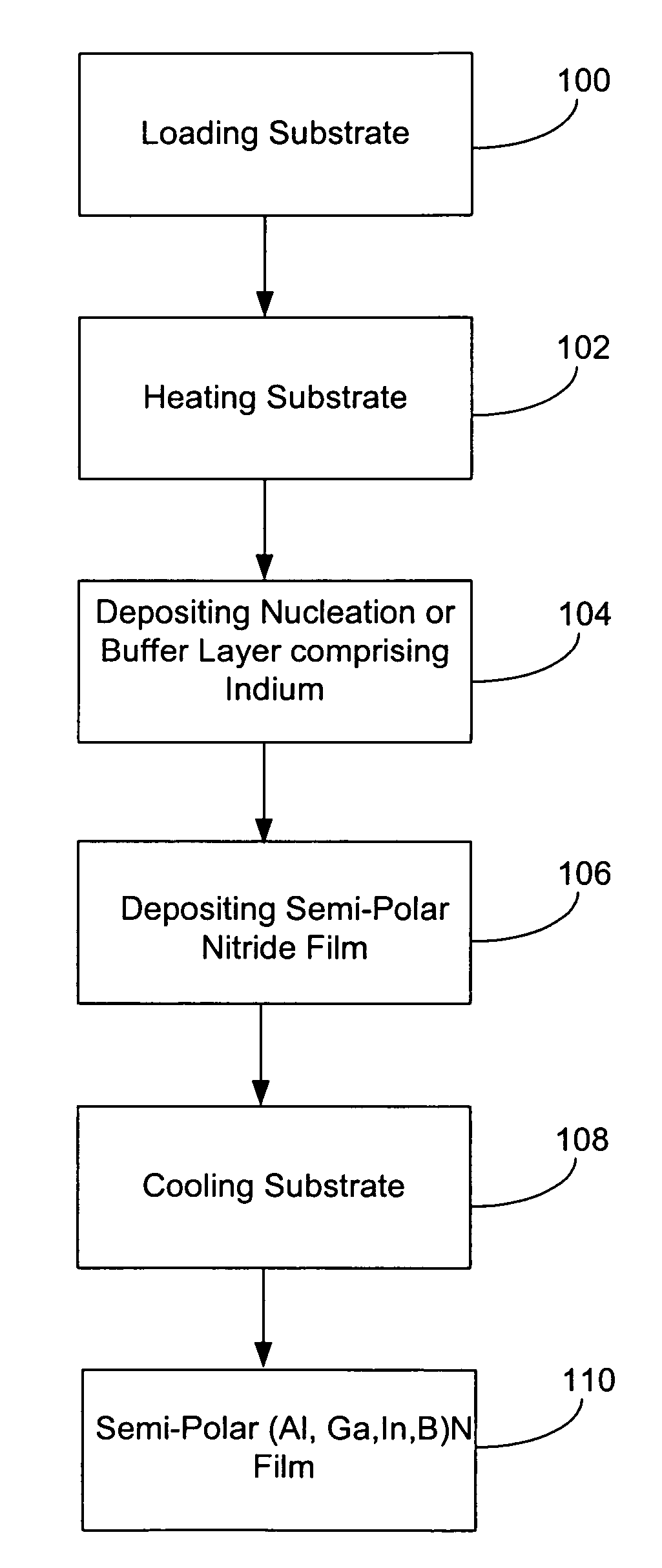
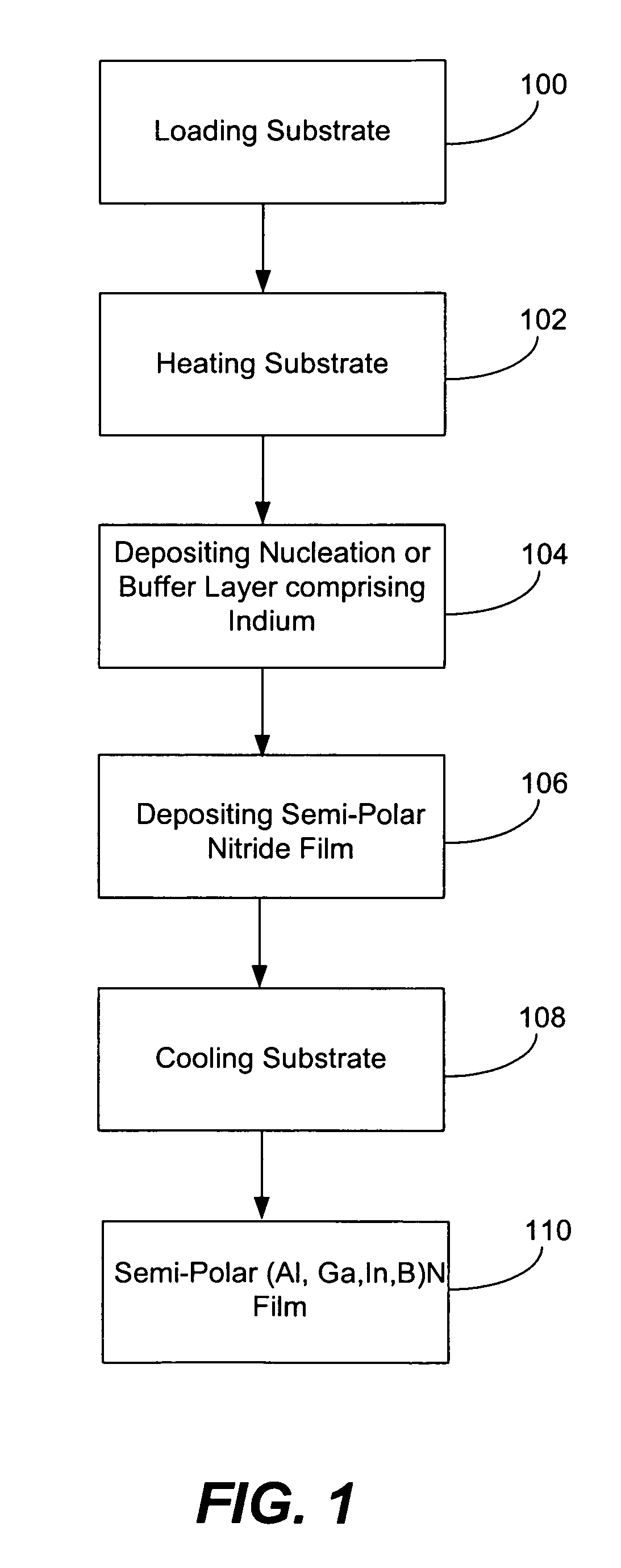
[0041] The present invention describes a method for growing device-quality planar semipolar (e.g. {11 22} plane) nitride semiconductor thin films via MOCVD by using an (Al,In,Ga)N nucleation layer containing at least some indium. Growth of semipolar nitride devices on planes (for example, the {11 22} and {10 13} planes of GaN), offers a means of reducing polarization effects in würtzite-structure III-nitride device structures. The term “nitrides” refers to any alloy composition of the (Ga,Al,In,B)N semiconductors having the formula GanAlxInyBzN where 0≦n≦1, 0≦x≦1, 0≦y≦1, 0≦z≦1 a...


PUM

PropertyMeasurementUnit
temperatureaaaaaaaaaa
pressureaaaaaaaaaa

Abstract

A method for enhancing growth of device-quality planar semipolar nitride semiconductor thin films via metalorganic chemical vapor deposition (MOCVD) by using an (Al,In,Ga)N nucleation layer containing at least some indium. Specifically, the method comprises loading a substrate into a reactor, heating the substrate under a flow of nitrogen and/or hydrogen and/or ammonia, depositing an InxGa1−xN nucleation layer on the heated substrate, depositing a semipolar nitride semiconductor thin film on the InxGa1−xN nucleation layer, and cooling the substrate under a nitrogen overpressure.

Description

CROSS-REFERENCE TO RELATED APPLICATIONS [0001] This application claims the benefit under 35 U.S.C. Section 119(e) of the following co-pending and commonly-assigned U.S. patent application: [0002] U.S. Provisional Patent Application Ser. No. 60 / 760,628 filed on Jan. 20, 2006, by Hitoshi Sato, John Kaeding, Michael Iza, Troy J. Baker, Benjamin A. Haskell, Steven P. DenBaars and Shuji Nakamura entitled “METHOD FOR ENHANCING GROWTH OF SEMIPOLAR (Al,In,Ga,B)N VIA METALORGANIC CHEMICAL VAPOR DEPOSITION”, attorneys docket number 30794.159-US-P1 (2006-178); [0003] which application is incorporated by reference herein. [0004] This application is related to the following co-pending and commonly-assigned application: [0005] U.S. Utility patent application Ser. No. 11 / 372,914 filed Mar. 10, 2006, by Troy J. Baker, Benjamin A. Haskell, Paul T. Fini, Steven P. DenBaars, James S. Speck, and Shuji Nakamura, entitled “TECHNIQUE FOR THE GROWTH OF PLANAR SEMI-POLAR GALLIUM NITRIDE,” attorneys docket n...

Claims


Application Information

Patent Timeline
Patent Type & Authority Applications(United States)
IPC IPC(8): H01L21/20
CPCC30B25/02C30B29/403C30B29/406H01L21/0242H01L21/02433H01L29/045H01L21/02502H01L21/02516H01L21/0254H01L21/0262H01L21/02365H01L21/02458H01L21/20
Inventor SATO, HITOSHIKAEDING, JOHN F.IZA, MICHAELBAKER, TROY J.HASKELL, BENJAMIN A.DENBAARS, STEVEN P.NAKAMURA, SHUJI
Owner RGT UNIV OF CALIFORNIA
Why Eureka
Try Eureka